
Switching power supply monolithic switching regulator DN-25 configuration
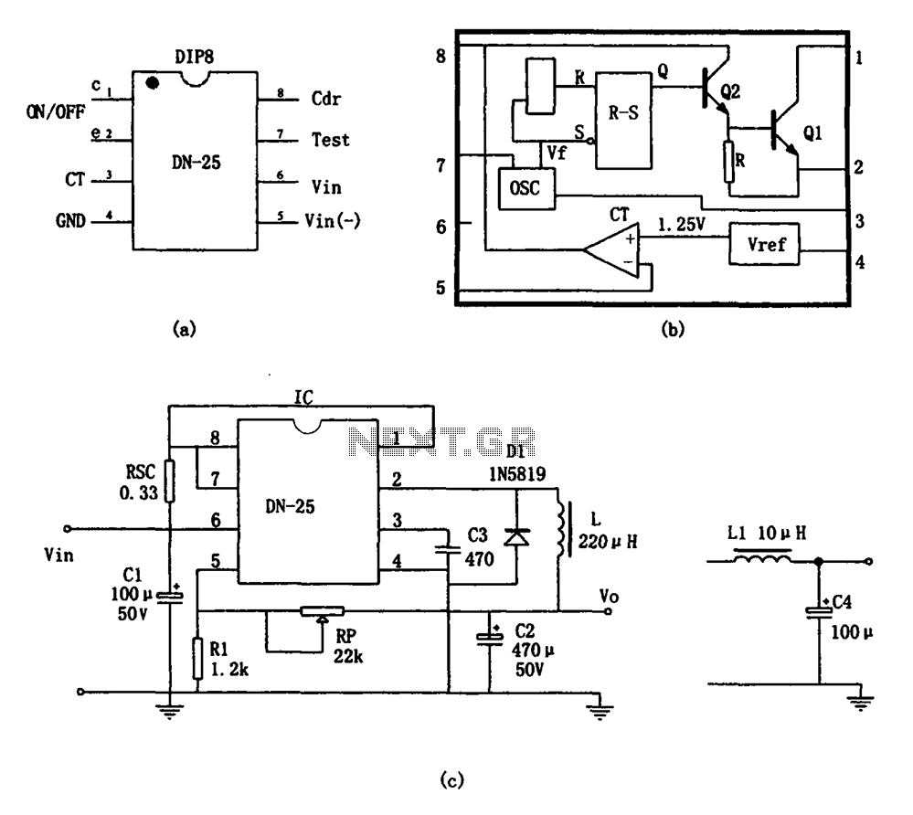
The DN-25 IC switching power supply is designed for applications requiring reliable and efficient voltage regulation. The device operates over a broad input voltage range, making it versatile for various applications. The adjustable output voltage allows for customization based on specific requirements, making it suitable for a wide range of electronic devices.
The internal architecture of the DN-25 is pivotal for its functionality. The oscillator generates a pulse-width modulation (PWM) signal, which is critical for controlling the output voltage. The RS flip-flop plays a significant role in maintaining the stability of the output frequency, ensuring that the output pulse maintains its desired characteristics. The Darlington pair configuration at the output stage allows for higher current gain, facilitating the delivery of the maximum output current of 1A.
The voltage reference and comparator are essential for achieving precise voltage regulation. By adjusting the feedback through the inverting input of the comparator, the output voltage can be finely tuned. This feature is particularly important in applications where voltage stability is crucial.
The performance metrics of the DN-25 demonstrate its efficiency and reliability. An efficiency rating of 82.50% indicates effective power conversion, minimizing energy loss. The load regulation of 0.03% suggests that the output voltage remains stable under varying load conditions, while the short-circuit current limit protects the circuit from damage during fault conditions.
In applications where ripple voltage can affect performance, the addition of an LC filter can significantly enhance output stability. This filter smooths the output waveform, reducing the ripple to acceptable levels for sensitive electronic components.
Overall, the DN-25 IC represents a robust solution for switching power supply applications, combining flexibility, efficiency, and reliability in a compact package. As shown in FIG by DN-25 IC switching power supply. DN-25 is a monolithic switching power supply device, suitable for the production of medium output current, wide voltage rang e power supply. Its main performance indicators are as follows: Input voltage VIN 3 ~ 40V, output voltage Vo 1.25 ~ 24V (adjustable), the maximum output current IOM 1A, the maximum output power POM 36W, load short-circuit current limit IOSH 1.1A. DN-25 8-pin double-line package (DIP-8), the internal circuit includes: (1) an oscillator (OSC); (2) RS flip-flop; (3) output switch; (4) Voltage reference (VREF 1.25V) and a comparator.
DN-25 internal oscillator frequency f foot accessed by the timing capacitor CT decision, f 1/CT.When turned on, the oscillator start-up, the output signal by the RS flip-flop VF converting plastic to produce a frequency to maintain the original, rectangular pulse excitation voltage, after the Darlington circuit and then by Q1, Q2 composed amplified by the output pin. Adjust the output voltage V0 is achieved by adjusting the voltage comparator inverting input pin can be realized.
Change pin voltage can be adjusted RS flip-flop output excitation pulse width to cause a change in the output voltage Vo. The power supply VIN 25V, Vo (1 + RP/R) VREF, stability is 0.12%; load regulation of 0.03%; short-circuit current limit IOSH 1.1A; efficiency 82.50%; ripple is less than 120mVp-p.
To further reduce the ripple, you can add a section LC filter at its output.
Related Circuits
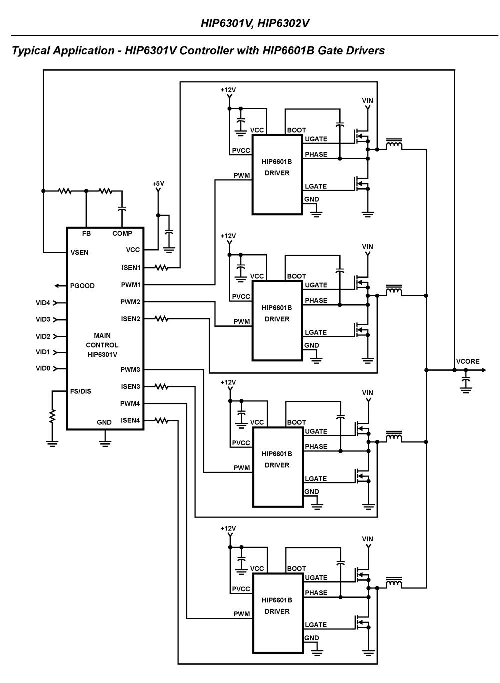
The HIP6301V and HIP6302V control the microprocessor core voltage regulation by driving up to four synchronous-rectified buck channels in parallel. The multiphase buck converter architecture employs interleaved timing to increase ripple frequency and minimize input and output ripple currents....
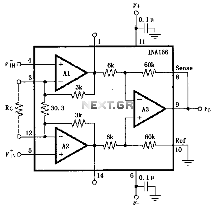
The basic connection circuit for the INA166 includes signal and power connections. A 0.1 µF tantalum capacitor should be used for filtering the chip's power supply terminal, and the PCB layout should be designed to position this capacitor as...
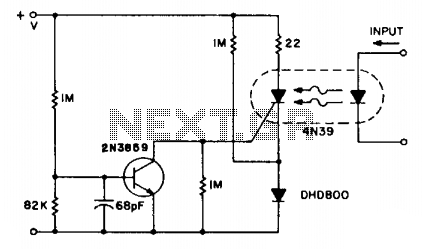
The SCR coupler circuit offers increased sensitivity to input signals as demonstrated. This enables the utilization of the more economical 4N39 (H11C3) with the drive currents exceeding 7 mA provided by the input circuit. The SCR coupler circuit is designed...
When the amplifier is installed inside the suitcase, it will require a change to stop working. The LA47536 has a control pin (pin 4) that requires a small voltage of up to 2V to turn on the amplifier. Transistors...
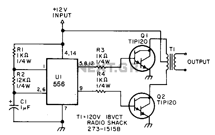
This low-power inverter utilizes only nine components to convert 10 to 16 VDC into a 60 Hz, 115 V square-wave output suitable for operating AC equipment with a maximum power of 25 W. The initial section of the 556...
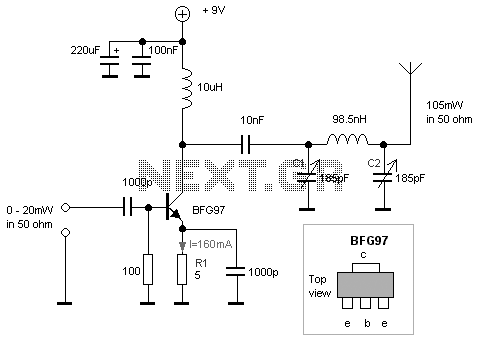
This page investigates a simple PA for 50MHz. This power amplifier will boost a low-level signal about 10-20mW to over 100mW. The power consumption will yet be quite low. At the bottom of this page, a complete transmitter based...