
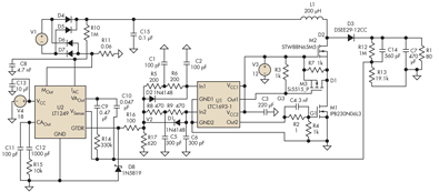
Switchmode Power Supply For Car Audio

Switching power supplies are essential components in modern electronic circuits, providing efficient voltage conversion and regulation. They operate by rapidly switching the input voltage on and off, which allows for energy transfer through inductors and capacitors, thus maintaining high efficiency and reducing heat generation compared to linear power supplies.
A basic schematic of a switching power supply typically includes several key components: an input filter, a switching element (such as a MOSFET), a transformer or inductor, a rectifier, and an output filter. The input filter is designed to smooth out the incoming voltage and protect the circuit from voltage spikes. The switching element is controlled by a pulse-width modulation (PWM) signal, which determines the duty cycle and, consequently, the output voltage.
The transformer or inductor plays a critical role in energy transfer and voltage transformation. In a flyback converter configuration, for instance, energy is stored in the magnetic field of the transformer during the "on" phase of the switching element and released to the output during the "off" phase. The rectifier then converts the alternating current (AC) output from the transformer into direct current (DC), which is further smoothed by the output filter to provide a stable voltage to the load.
Feedback mechanisms are often incorporated to regulate the output voltage, ensuring that it remains constant despite variations in input voltage or load conditions. This can be achieved through various methods, including voltage sensing and error amplification.
Understanding the operation and design principles of switching power supplies is crucial for developing efficient and reliable electronic systems. This project serves as a foundational reference for those looking to delve deeper into the field of power electronics.This contributed project is a result of considerable collaboration between Sergio and myself, and should not be seen as necessarily a complete project in itself, but a stepping stone to understanding switching power supplies, how they work, and what you can do with them. 🔗 External reference
Related Circuits
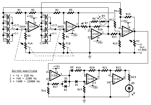
This oscillator generates low-distortion sine waves within a frequency range of 16 to 22,000 Hz. The sine wave oscillator is designed to produce high-quality sine wave outputs with minimal distortion across a wide frequency spectrum. The operational range of 16...
The frequency of this sine-wave oscillator is determined by a direct voltage, U, ranging from 0 to 15 V. The distortion in output signals of up to 10 Vpp does not exceed 1%. When the output is reduced using...
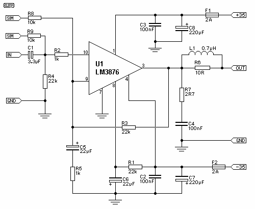
The supply voltage should be about +/- 35 Volts at full load, which will let this little guy provide a maximum of 56 Watts (rated minimum output at 25 degrees C). To enable maximum power, it is important to...
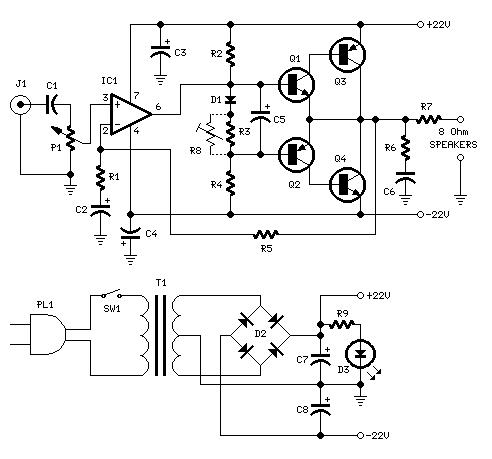
Power amplifier circuit diagram using the IC TLE2141C. The TLE2141C is a low-noise, high-voltage, high-slew-rate operational amplifier with a frequency response of 30 Hz. The TLE2141C operational amplifier is designed for applications requiring high precision and low noise, making it...
The mechanical and electrical schematic in Figure 5 illustrates a simple circuit comprising several components. The first component is an electronic crossover section utilizing the NE5532 operational amplifier, which is known as the "Emperor of the op-amp." This section...
Adding a discharge path to the upper MOSFET of a cascode circuit significantly reduces the unavoidable Miller effect, thereby enhancing the Power Factor Correction (PFC) performance of a power supply's front end. In a cascode configuration, the upper MOSFET is...