
TALKING ELECTRONICS BEC

This is called OUT OF PHASE signals and you cannot connec t the output directly to the input to get the transistor to oscillate. If you do, the rising output will be fed into the base to turn the transistor ON and this will reduce the output. The signal has to be delayed by a short period of time to allow the output voltage to rise and then the transistor can be turned ON to reduce the voltage on the output.
This delay is created by a set of capacitors and resistors on the base. We have already mentioned the fact that a capacitor takes a period of time to charge and this feature is utilized in the PHASE-SHIFT OSCILLATOR circuit. The value of the components create a time-delay and this sets the frequency at which the circuit operates.
But it`s a bit more complex than a single "time-delay" arrangement. Each capacitor is doing something different at each part of the cycle. The interesting point to note is the feedback signal only has to be about 1/50th of the collector signal for the circuit to operate as the gain of the transistor is about 50 to 100. This means there can be a lot of ATTENUATION (reduction) in the signal and the circuit will still operate.
The signal through the 1M finds it difficult to pull the base up or down "quickly" because the 22n capacitor has a very large "holding effect" on the signal. This voltage is passed to the three uncharged capacitors and they pull the base up very quickly to turn the transistor ON.
The secret to the operation of the circuit is the voltage across the second 10k resistor. During this time the voltage across it is 0. 7v and this reduces slightly as the first capacitor charges, so that the "hard turn-on" of the transistor is reduced. The collector voltage is allowed to gradually rise and as the charge on the first two capacitors increases, the charging current reduces and this means the voltage across the second 10k resistor reduces.
This reduction in voltage is passed to the base of the transistor via the 3rd 22n capacitor and the transistor turns off a little. The 1M base-bias resistor now comes into operation by turning the transistor ON and the collector voltage falls.
The "falling effect" is passed directly to the base via the three capacitors with the result that they turn the transistor off slightly. The 1M takes over by charging the 22n and this controls the rate at which the transistor turns off. As you can see, the operation of the circuit is much more complex than explained in any text book and its important to know exactly what is happening so that when you look at the waveform on a CRO, you understand how the waveforms are produced.
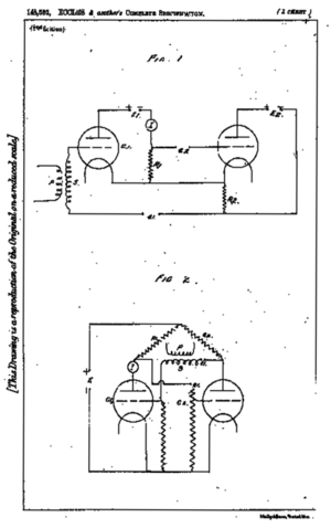
The animation above showsthe output voltage of the Phase shift oscillator is rising and falling. We have already seen a rising and falling voltage produces a sinewave as shown in the diagram opposite. This is how a rising and falling voltage produces a sinewave. Another circuit that produces a sinewave is the Colpitts Oscillator. It is recognised by a small capacitor tapping the TUNED CIRCUIT to monitor the waveform. The colpitts oscillator consists of a tuned circuit made up of inductor L1 and capacitor CT (sometimes called the tuning capacitor) and a transistor in common-base mode.
At the frequency of operation for the circuit, the capacitor C1 on the base of the transistor prevents the base moving (rising and falling) and this puts it in the common-base configuration. Re is the emitter resistor and keeps the emitter from the 0v rail so the emitter can be injected via capacitor Cf (the feedback capacitor) to keep the oscillator operating.
This is an amazing effect for two seemingly simple com 🔗 External reference
Related Circuits
A flip-flop is a bistable multivibrator. It is a circuit that has two output states and is switched from one to the other by means of input signals. A flip-flop serves as a fundamental building block in digital electronics, primarily...
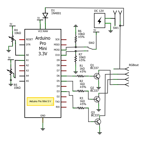
There are numerous LED flasher projects available on the internet, some of which are designed for low current consumption. However, the requirement was for an extremely small flasher suitable for geocaching that could last at least one year using...
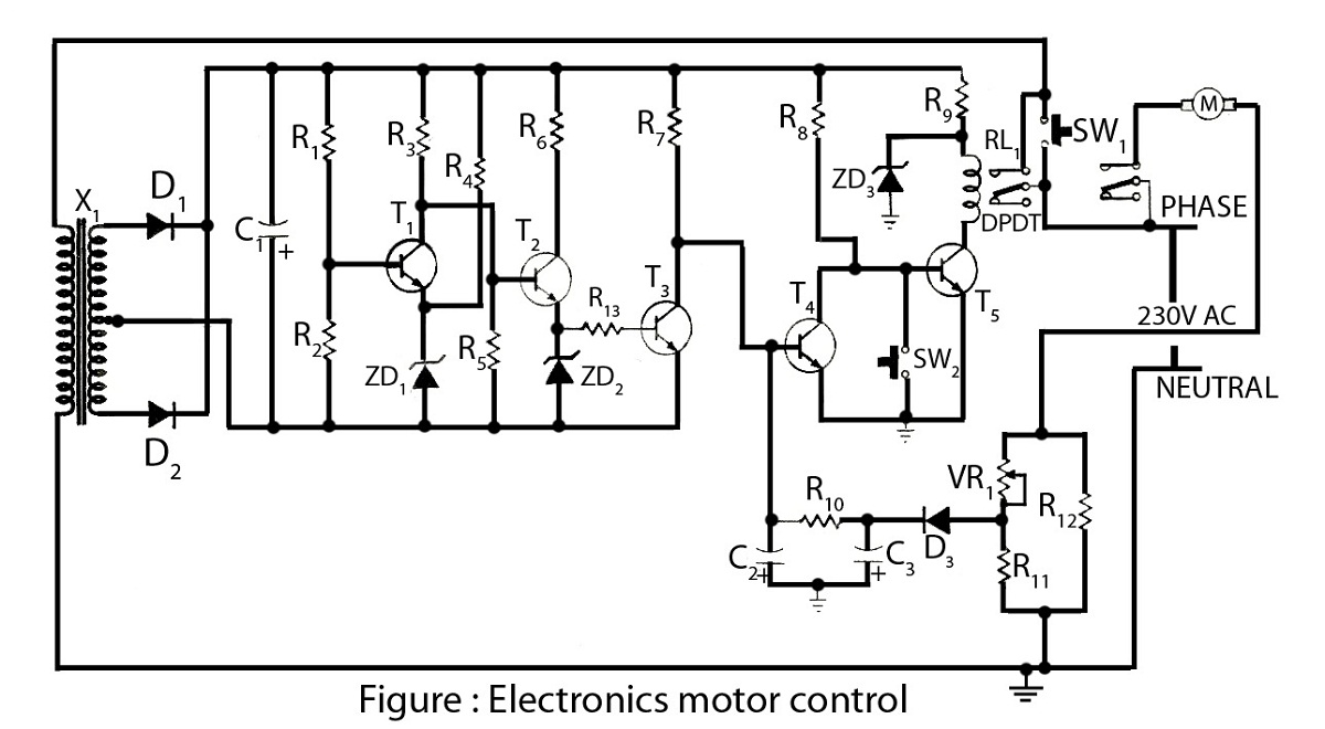
Electronics motor control is a simple circuit made without an integrated circuit (IC). It involves the electronic control of an AC motor and includes a circuit diagram along with a description of the electronics motor controller. The electronics motor control...
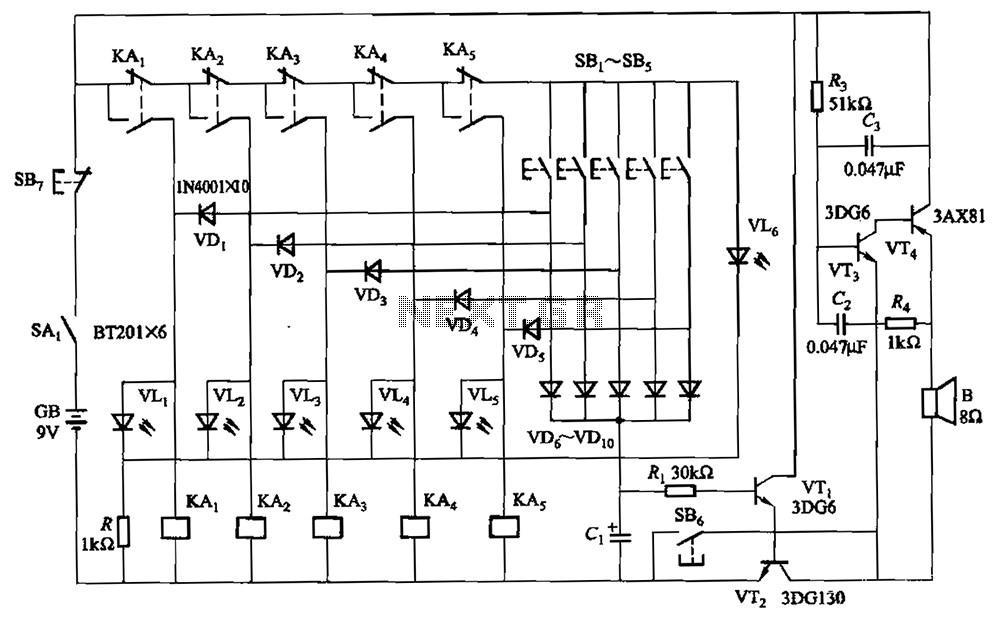
A relay-style circuit designed for a five electronic responder group. This circuit features self-locking capabilities, sound and light displays, time monitoring, and additional functions. The circuit includes a monitoring time button operated by the moderator. When this button is...

These items were sold nationally several years ago. The fish would sing, open its mouth, turn its head, and flap its tail. After removing the back panel, all of the existing electronics were removed leaving only the 3 servo...
The circuit is a high-power car audio amplifier schematic. It functions as a car audio amplifier using the PA02 and LH0101 integrated circuits (ICs). Each IC delivers an output power of 30W with an 8-ohm impedance. The part list...