
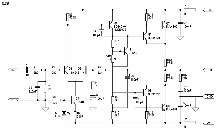
TDA8920BTH 200 watts d class amplifier circuit diagram

The TDA8920BTH is a highly efficient Class D audio amplifier IC, capable of delivering substantial power while maintaining low thermal dissipation. The design allows for a dual output configuration, providing 100 watts per channel in a stereo setup, making it suitable for various audio applications including home theater systems and professional audio equipment.
The amplifier operates within a voltage range of ±12.5 V to ±30 V, which allows for flexibility in power supply selection. The quiescent current, which is the current consumed when the amplifier is idle, is notably low, enhancing overall energy efficiency and reducing heat generation during operation.
The input stage of the amplifier is crucial as it converts the analog audio signal into a digital format. This conversion is achieved using a PWM modulator, which encodes the audio signal into a series of pulses that represent the amplitude of the audio waveform. The PWM technique allows for high fidelity reproduction of audio signals while minimizing distortion.
Following the PWM modulation, the digital signal is processed by a control and handshake block, which ensures that the output stage operates correctly and safely. This block coordinates the timing and operation of the driver circuits, which are responsible for controlling the high-side and low-side output transistors. The synchronization of these transistors is essential for efficient power delivery and to prevent crossover distortion, a common issue in amplifier designs.
Overall, the TDA8920BTH Class D audio amplifier represents a sophisticated solution for high-power audio amplification, combining efficiency, low heat generation, and high output capabilities, making it an ideal choice for robust audio applications.This high power class D audio amplifier electronic project is designed using the TDA8920BTH audio power amplifier IC. This power amplifier audio IC has a very high efficiency with very low dissipation, providing a very high output power.
The typical output power is 200 watts ( 2 x 100 W). The TDA8920BTH 200 watts d class amplifier operates over a wide supply voltage range from ±12. 5 V to ±30 V ( ±32 V non operating) and consumes a very low quiescent current. The audio input signal of this 200 watts d class amplifier is converted into a digital pulse width modulated signal via an analog input stage and Pulse Width Modulation (PWM) modulator. To enable the output power transistors to be driven, this digital PWM signal is applied to a control and handshake block and driver circuits for both the high side and low side.
🔗 External reference
Related Circuits
The basis for this amplifier has been around now for several years as Project 3A, and requires only relatively small modifications to be able to operate in Class-A. The biggest change is in output power (reduced dramatically from the 60-100W...
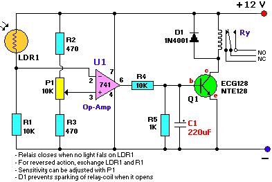
The schematic diagram has been modified to include a 220µF smoothing capacitor connected between the base of transistor Q1 and ground. This addition effectively mitigated the issue of relay chatter, which involved rapid on/off switching at light levels. The...
The music equalizer display schematic is relatively straightforward to construct. It can be assembled on a compact breadboard, utilizing the components listed previously. Due to the high number of connections required, it is advisable to have an ample supply...
A real-time controller is a device designed to continuously manage household devices, both in real-time and according to a predetermined schedule. This article focuses on a series of real-time controllers utilizing the AT89C2051 microcontroller, which serves this purpose effectively....
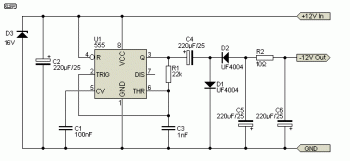
This is a voltage doubling circuit built using the well-known timer IC 555. The circuit is straightforward and easy to construct. The construction is not critical. Rectifier diodes should be ultrafast (such as UF4004 or similar), or 1N4148 signal...
Any ideas? Is this circuit going to be standalone? Is there any other circuitry around it, perhaps a microcontroller? What circuitry does the timing device contain, or does it even contain electronics? Abdullah Kahraman Mar 22, '13 at 18:10....