
TDA8932B D Audio Amplifier

The TDA8932B/33(B) is a powerful audio amplifier designed to operate efficiently under single-supply conditions, making it suitable for various applications where space and power conservation are critical. The integration of half-supply voltage buffers simplifies the circuit design by eliminating the need for external components to generate the necessary reference voltages, thus reducing the overall component count and enhancing reliability.
In this configuration, the first buffer connected to the reference decoupling capacitor (Chvpref) stabilizes the HVPREF pin, ensuring that the amplifier operates within its optimal range. This reference voltage is crucial for maintaining consistent performance and reducing noise in the audio output.
The two additional buffers serve to manage the AC-coupling capacitors (Cse), which are essential for blocking DC voltage while allowing AC audio signals to pass through to the speaker. By using these buffers, the circuit can effectively handle the audio signal without distortion, providing a clear and high-quality sound output. The careful arrangement of these components within the circuit diagram illustrates a well-structured approach to achieving efficient audio amplification in a compact design.
Overall, the TDA8932B/33(B) circuit exemplifies a modern solution for audio amplification, combining advanced integration with practical design considerations for single-supply applications.The following circuit diagram is a simplified application circuit of the TDA8932B/33(B) device when operated from an asymmetrical supply (single supply). Here`s the circuit diagram: To simplify the design for an asymmetrical supply in SE configuration, the TDA8932B/33(B) is equipped with three integrated half supply voltages buffers.
The first buf fer is for the reference decoupling capacitor (Chvpref) on HVPREF (pin 11) and the rest (two other buffers) are for the two AC-couple capacitors (Cse) in series with the speaker. [Source: NXP Application Note] 🔗 External reference
Related Circuits
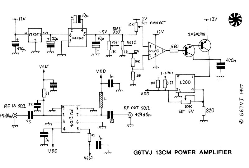
A simple synthesized 13 cm ATV exciter has led to considerations for an appropriate power amplifier. The exciter generates approximately 10 mW, which may be sufficient to drive a MMIC or hybrid amplifier. However, at 2.3 GHz and higher...
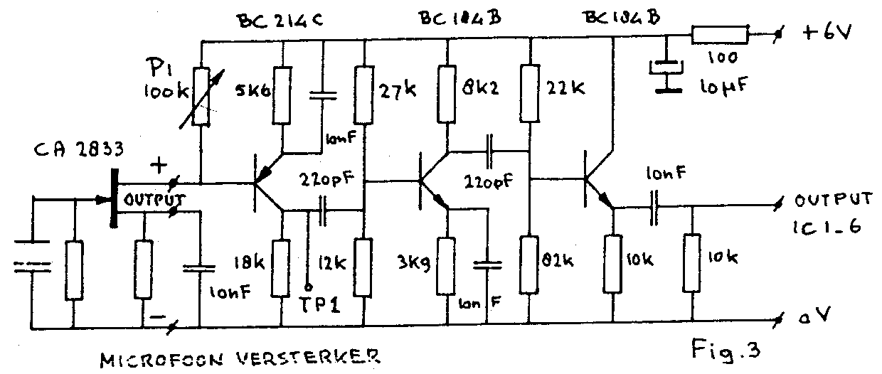
The microphone has high sensitivity in the audio range, but in the ultrasonic range, the sensitivity decreases rapidly. The receiver is very sensitive. To prevent overdriving and feedback due to the high sensitivity of the microphone in the audio...
The microphone preamplifier circuit design presented in this schematic utilizes the SSM2015 component manufactured by Precision Monolithics Inc. (PMI). This component provides high amplification with low noise characteristics (1.3nV/f). The design is configured to handle differential input signals and...
This project utilizes the IRF510 MOSFET, a widely available N-Channel enhancement mode power field effect transistor. It is designed to withstand specified levels of energy in breakdown avalanche mode. Unlike bipolar transistors, which are current-controlled and have lower input...
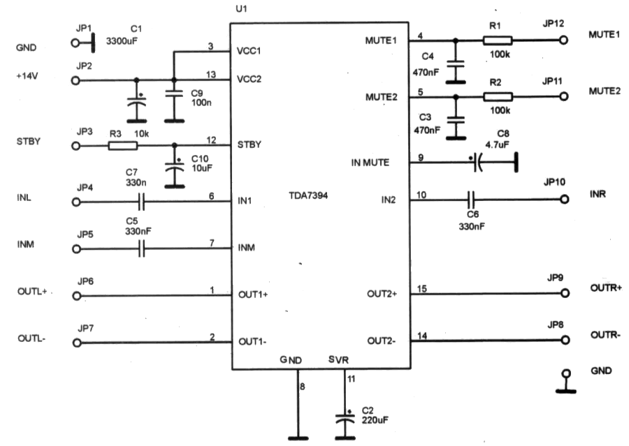
This car audio stereo amplifier can deliver up to 30W to each speaker and is built with the TDA7394 from the Philips TDA7394 datasheet. The TDA7394 is a high-performance car audio amplifier designed to drive speakers with an output power...

A VU (Volume Unit) meter has traditionally been a key component of audio metering systems. The Peak Program Meter (PPM) is known for its inadequacy in accurately displaying peak signal levels. This circuit serves the same function as previously...