
Telephone Hold Line
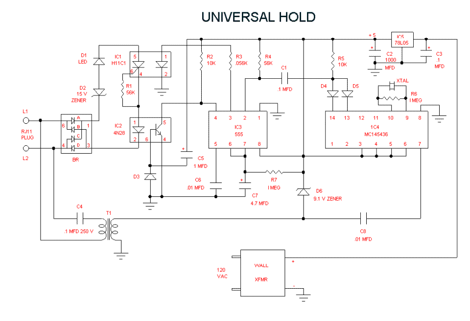
The UNIVERSAL HOLD circuit is designed to maintain the telephone line in a state that simulates an off-hook condition even after the physical handset is hung up. This is achieved through the detection of a specific DTMF tone, specifically the tone generated by the pressing of the # key. The circuit employs a bridge rectifier (BR) to ensure that it is not polarity sensitive, allowing for flexible connections to the telephone line. The rectifier directs the voltage appropriately to various components, including a zener diode (D2) and an integrated circuit (IC2), which plays a crucial role in the operation of the hold function.
The SCR within optoisolator IC1 is pivotal for maintaining the hold condition. Once triggered by the LED current, it remains in a conductive state until the anode voltage is removed, making it ideal for this application. The circuit is designed to detect changes in the line voltage that occur when a phone is picked up or hung up. When a phone is off-hook, the line voltage drops significantly, which subsequently disables the hold function.
The tone decoder IC4 is integral in recognizing the DTMF signal corresponding to the # key. It generates a hexadecimal output that is processed by a logical AND circuit to confirm the presence of the correct tone. The timing mechanism, controlled by timer IC3, ensures that the hold function can be initiated and maintained for a specific duration, allowing for user flexibility.
The circuit is also designed with safety features, including transient protection via zener diode D6, and it incorporates an optoisolator (IC2) that not only helps in resetting the timing cycle but also provides isolation between the telephone line and the rest of the circuit, ensuring safe operation.
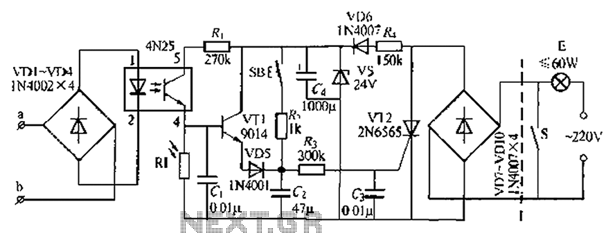
Overall, the UNIVERSAL HOLD circuit is a sophisticated solution for managing telephone line states, utilizing DTMF detection, timing control, and robust isolation techniques to provide a reliable hold function.The UNIVERSAL HOLD circuit detects the dual tone, multi frequency (DTMF) tone that is generated when the # key is pressed and then activates a circuit that partially loads the telephone line so that the central office thinks a phone is still off hook even after it is hung up. When any phone is again picked up, the hold function is canceled. Figure 1 shows the schematic diagram of the UNIVERSAL HOLD circuit. The telephone line is connected to the hold components through bridge rectifier BR so the input is not polarity sensitive and the input lines may be connected either way. BR always connects the positive side of the line to zener diode D2 and the negative side of the line to IC2.
If L1 is positive, current flows into the circuit through bridge diode A and back out through diode D into L2. If L2 is positive, current flows in through diode C and out through diode B into L1. The telephone line also connects to tone decoder IC4 through C4 and T1. Optoisolator IC1 contains a silicon controlled rectifier (SCR) having a characteristic that makes it continue to conduct current, or latch on, once turned on by current flowing through an optically coupled LED within the IC.
The SCR conduction continues even after the LED current is removed, providing enough anode current is available to sustain it. When the SCR anode voltage is removed and conduction stops, it will not resume when voltage is re-applied until again triggered by LED current.
This characteristic makes the SCR optoisolator ideal for a line hold application. When all phones are hung up (on-hook) the voltage across the telephone line is about 48 volts. When a phone is picked up (off-hook) it places a load on the line and a current of about 20 milliamps flows through the phone which causes the line voltage to drop to about 3 to 8 volts, depending on the telephone unit. Current also flows through circuits in the central office, indicating that the phone has been picked up.
A call is put on hold when all phones are hung up and the SCR in IC1 is triggered on by circuits driving its LED (we’ll tell you more about this later). When The SCR conducts, current flows through BR, D2, D1, IC1, IC2 and back through BR, placing a load on the line that keeps the central office circuits active.
A 15 volt drop across D2, a 2 volt drop across D1, a 1.5 volt drop across the LED in IC2 and about a 1.5 volt drop across the diodes in BR results in the normal 48 volt open circuit line voltage across L1, L2 being clamped to about 20 volts which allows line current to flow but is a higher voltage than when a telephone loads the line. Now when a phone is picked up and the line voltage drops to about 8 volts or less, there is no longer enough voltage to produce conduction through D2, D1 IC1, IC2 and BR and the hold function is canceled.
LED D1 is provided to indicate that a call is on hold. The telephone line also connects through C4 and transformer T1 to capacitor C8 which couples the DTMF signal to the input of IC4, a Motorola MC145436 or Harris CD22204 dual tone, multi frequency tone decoder integrated circuit used to detect the # key tone. The 3.57 Mhz crystal XTAL generates a clock required by the decoder. Zener diode D6 clamps its input to prevent damage from transients. The decoder has four outputs that produce a hexadecimal code corresponding to the tones it receives when a key is pressed as shown in table 1.
When these outputs are further decoded, the 1” or 0” status of all four outputs usually must be considered to get a unique hexadecimal number for each DTMF tone. Notice, however, that a 1” occurs simultaneously in both the pins 13 and 14 outputs only when the # key is pressed.
This makes using the outputs easier since only two hexadecimal bits must be considered to decode the # key. The binary decoding is done by a logical AND circuit consisting of two diodes, D4 and D5 whose cathode terminals must both be at an up level or logical 1” for their anodes, which are connected together, to be pulled up by R5.
This up level discharges C1 through R4 into the positive supply. When the # key is released the DTMF signal stops, pins 13 and 14 go down again and a down level pulse is produced by time constant C1, R4 at the pin 2 trigger input of timer IC3. Since the IC3 trigger input must receive a negative transition to start a timing cycle, the cycle does not start until the # key is released.
When the timing cycle starts, IC3 output pin 3 goes up for five seconds and drives current through R3 into the LED within IC1 which places its SCR in a potentially conducting state where it needs only to have sufficient voltage applied to its anode terminal to make it heavily conduct and latch on, a condition that occurs when the phone is hung up. The five second output from IC3 keeps IC1 LED current flowing long enough to hang up the phone and have the required anode voltage applied to maintain conduction.
The time duration is controlled by R7 and C7 and may be altered by changing the value of R7. IC2 is an optoisolator with a transistor output. After the # key is pressed and the phone is hung up, telephone line current flowing through the led in IC2 turns its transistor on which resets timer IC3 and terminates its timing cycle. This reset function removes current from the LED in IC1 and allows a hold to be canceled immediately after initiating it without having to wait for the five second cycle to complete.
The transistor within IC2 also performs a power-on reset by having its base coupled through C5 to the positive supply. When power is turned off C5 discharges through D3. Power is supplied by a 12 volt DC wall transformer and by IC5, a 78L05 5 volt regulator, and is filtered by C2 and C3.
The power supply, DTMF decoder and timing circuits are isolated from the telephone line by the optoisolators and transformer T1. 🔗 External reference
Related Circuits
Most analog multimeters can measure resistance across a wide range of values; however, they can be inconvenient due to their reverse reading scale, which is also non-linear. This can lead to poor accuracy, especially at the high-value end of...
Electronic FM Telephone Transmitter Schematic. The following schematic design illustrates a circuit diagram for an FM telephone transmitter built on a compact PC board layout. This small design allows it to be easily integrated within the housing of a...
The CX9800 models of mobile phones and desktop PCs feature a high-performance voice processing circuit that compresses the amplitude and bandwidth of the microphone signal. This design enhances the sensitivity of the microphone and its adaptability to varying distances....
An automatic light system is integrated with a telephone block system. When the phone rings, the owner is prompted to pick up the handset or pull a lever, causing the lamp to light up. If there is no contact...
Additionally, it may be necessary to include another input capacitor to mitigate high-frequency noise, although this is not directly related to the main question. The objectives are to achieve a voltage output of 0 - 12 V with a...
After constructing a Pulse Width Modulator for high-power LEDs, another LED modulator was developed for an optical transceiver. This project utilized a different approach, focusing solely on linear techniques for audio modulation. Similar to the PWM circuit, this circuit...