
Telephone transmitter
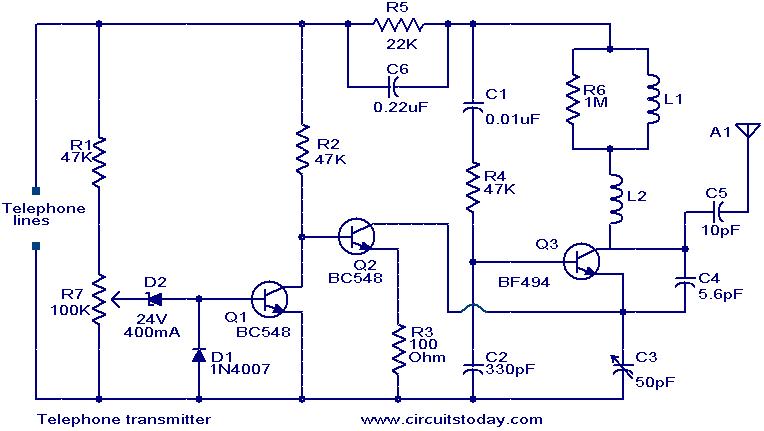
This circuit operates by leveraging the voltage levels present in a telephone line to control the state of multiple transistors, thereby facilitating the transmission of audio signals. The initial condition, with the telephone receiver on-hook, keeps the system idle as the high voltage allows for the stabilization of the circuit. The adjustment of resistor R7 is crucial as it sets the operational threshold for the Zener diode D2, ensuring that it enters breakdown at the correct voltage level of 24.7 volts. This action allows for the conduction of transistor T1, which is pivotal in controlling the state of transistor T2.
When the telephone receiver is lifted off-hook, the significant drop in line voltage to approximately 11 volts results in the deactivation of transistor T1. This deactivation leads to the activation of transistor T2, creating a pathway for the DC current to flow into transistor T3. The role of transistor T3 is critical as it functions as a common emitter radio frequency oscillator, generating the necessary frequency for FM transmission. The modulation of the audio signal occurs at this stage, with the output being taken from the collector of transistor T3.
The output signal is then coupled to the antenna through capacitor C5, which serves to block any DC components while allowing the modulated RF signal to pass through. This arrangement ensures that the transmitted signal remains clear and free from interference from the DC biasing present in the circuit. Overall, this circuit effectively utilizes basic electronic components to create a functional FM transmitter capable of transmitting telephone conversations over radio frequencies.This is a simple, but very useful circuit that can be used to transmit telephone conversations. When the telephone receiver is on hook the voltage across the lines will be about 48 volts. The preset R7 is so adjusted to obtain a 24. 7 V across between the cathode of D2 and ground. At this voltage the Zener diode D2 will be in breakdown and the tran sistor T1 will conduct. This makes the transistor T2 OFF. When the receiver is off hook, the line voltage drops to about 11 volts. This makes the transistor T1 OFF and subsequently the T2 ON. The T2 in switched ON condition will provide a DC path for the transistor T3 used in the FM transmitter section. The transistor T3 is wired as a common emitter radio frequency oscillator. In simple words the transistor T2 serves as an ON/OFF switch for this oscillator. The modulated signal will be available at the collector of transistor T3 and the signal id fed to the antenna via capacitor C5.
🔗 External reference
Related Circuits
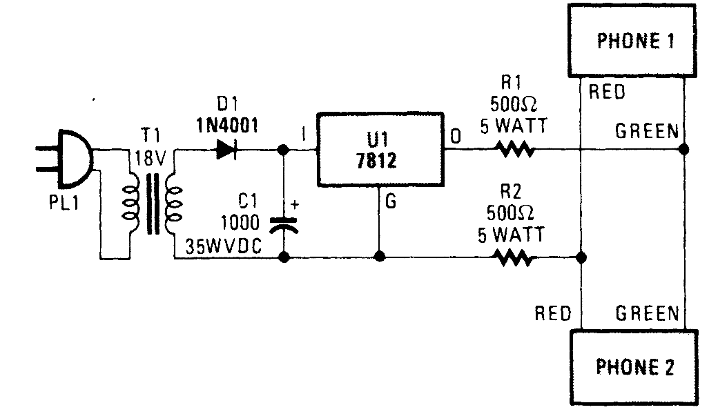
Tro telephones can be utilized as an intercom through the implementation of this circuit. Traditional rotary phones, particularly those that are non-electronic, may be the most effective for this purpose. Additionally, this method can also power handsets alone. The circuit...
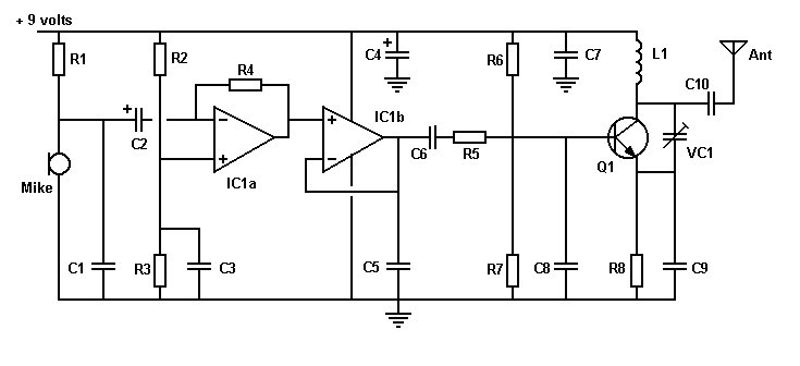
An FM transmitter circuit that utilizes a low power configuration, employing an operational amplifier as an audio preamplifier and a single transistor to function as the RF amplifier. This FM transmitter circuit is designed for low power applications, making...

The circuit diagram illustrates a simple long-range AM transmitter built using three transistors. With proper tuning and a compatible antenna, this transmitter can broadcast signals over a distance of up to 2 kilometers. The audio signal intended for transmission...
This circuit utilizes a sawtooth oscillator along with an output amplifier that drives a transistor. The components C1, C2, and L1 are essential for the oscillator's operation, forming a tank circuit that must be tuned to the resonant frequency....

This transmitter project is a highly efficient, rugged, and simple low-power continuous wave (C.W.) unit delivering more than 10W. It is crystal-controlled with stabilized high tension (H.T.) and features a buffer stage between the crystal oscillator and power amplifier...
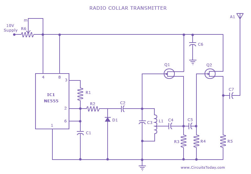
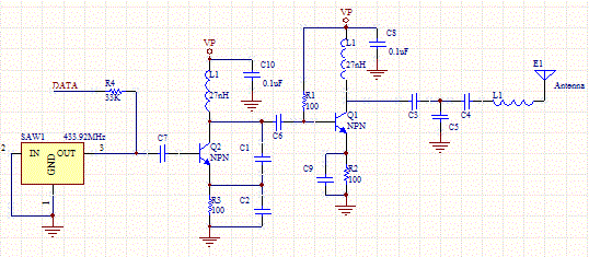
This is a radio transmitter circuit diagram designed for integration into radio collars using the NE 555 integrated circuit. The circuit transmits a pulse in the FM band, specifically between 88 MHz and 105 MHz. The radio transmitter circuit utilizes...