
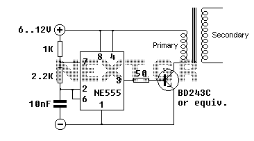
Tesla Coil using 555
Bipolar NPN transistor: BD243C
Casing: TO220
Max. collector current: 6 Amperes
Max. total power: 65 Watts, while case is at 25 degrees Celsius
Transition frequency: 3 MHz
hFE (current gain): 30 at 300mA (minimum value)
Following PCB design would make it easier to fit components on such a small space. Print it at 300 dpi to match the right scale. Otherwise, you should manipulate it to be printed in your specific printer resolution. You may refer to my PCB Design Page for more details on how to create your own PCBs. Lines that I painted thick are essential to carry enough current to the flyback through the power transistor, so do not thin them if you are going to draw it by hand, just like I do. Plate them with a solder layer to decrease conducting resistance. You may download a TIFF file already set to 300 dpi, ready to print.
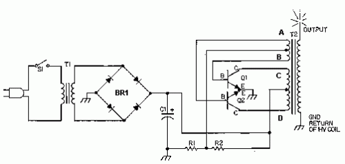
The described circuit operates as a single transistor flyback driver utilizing a 555 timer in astable mode. The use of the 555 timer allows for a stable operating frequency, which is crucial for maintaining the performance of the flyback transformer and ensuring the safety of the circuit. The circuit configuration includes two resistors (R1 and R2) and a capacitor (C) that determine the frequency and duty cycle of the output signal, which is fed into the base of a power transistor to control its switching behavior.
The selected component values of R1 = 1kΩ, R2 = 2.2kΩ, and C = 10nF are intended to achieve a theoretical frequency of approximately 27 kHz, with a duty cycle of 60% high and 40% low. These values can be adjusted to fine-tune the performance of the driver circuit, particularly by using a trimmer potentiometer in place of R2 to optimize the frequency and duty cycle for specific flyback transformer characteristics.
The power transistor, such as the BD243C, is chosen for its adequate specifications, including a maximum collector current of 6 Amperes and a maximum power rating of 65 Watts at 25 degrees Celsius. The transistor's transition frequency of 3 MHz ensures that it operates efficiently within the desired frequency range.
For PCB design, it is recommended to print the layout at 300 dpi to ensure proper scaling. The thick lines on the PCB layout are critical for carrying the necessary current to the flyback transformer, and care should be taken to maintain these dimensions if hand-drawing the circuit. A solder layer can be applied to improve the conductivity of these connections, enhancing the overall performance of the circuit. The availability of a pre-prepared TIFF file for printing further simplifies the process of creating the PCB. Single transistor flyback driver caused many problems due to it's operating principle. I received e-mails from people who were unable to get it functional even when they are sure that their flyback and transistor is OK. In addition, since it's resonance frequency is determined by every part of the system, when you try to draw an arc from the transformer, it changes dramatically in most of the cases.
Just because the operating frequency is important for the safety criteria, (both for mine and power transistor's), I decided to make it run on a constant frequency and built up another simple circuit, trying to stay in the specified limits of the 555 timer. Setting the operating frequency with an integrated timer is easy and practical. Following schematic is nothing more than the standard astable mode circuit design with a classic 555. It requires only two resistors and a capacitor to set frequency (with duty cycle of course) and another resistor to determine power transistor's base current, which you can find it's optimal value experimentally.
I used 1K for R1, 2.2K for R2, and 10nF for C which made circuit to run nearly at 27 kHz theoretically, at %60 high to %40 low duty cycle. You can quickly calculate operating parameters from the resistance and capacitor values with a small program that I've written.
Values given for R1, R2 and C in this diagram are the ones used on my prototype. You may change R1 and use a trimmer instead of R2 to find an optimum frequency / duty cycle combination for your flyback. By changing C, you'll have the ability to use higher or lower resistor values, but do not prefer too low resistances (especially for R1) for not to overload 555.
Power transistor is not critical and any other may be used as long as it's characteristics are equivalent or better. Here are the technical datas for BD243C for comparison: Bipolar NPN transistor : BD243C Casing : TO220 Max.
collector current : 6 Amperes Max. total power : 65 Watts, while case is at 25 degrees Celsius Transition frequency : 3 MHz hFE (current gain) : 30 at 300mA (minimum value) Following PCB design would make it easier to fit components on such a small space. Print it at 300 dpi to match the right scale. Otherwise you should manipulate it to be printed in your specific printer resolution. You may refer to my PCB Design Page for more details on how to create your own PCB's. Lines that I painted thick are essential to carry enough current to the flyback through the power transistor, so do not thin them if you gonna draw it by hand, just like I do...
Plate them with a solder layer to decrease conducting resistance. You may download a TIFF file already set to 300 dpi, ready to print. 🔗 External reference
Related Circuits
This project demonstrates how a capacitor can supply a pulse signal to a speaker. A capacitor is charged and then discharges its voltage to a speaker, which acts as a transducer that converts electrical signals into sound. The result...
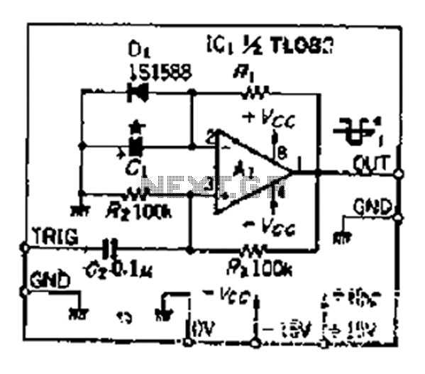
Although people believe that using a timer with an operational amplifier (op-amp) does not yield significant results, it can still be advantageous in certain scenarios. In environments with high noise levels, the application retains its benefits. When the phase...

This design circuit functions as an alarm system controlled by a keypad. The core component of the circuit is a single transistor from the BC547 series. The circuit requires a 12-key pad, which has 13 terminals; a matrix type...
The sections available in this datasheet cover general design considerations for the 555 timer, frequently asked application questions (FAQ), design formulas, and examples of innovative applications. Examples of applications include a Missing Pulse Detector, Pulse Width Modulation (PWM), Tone...
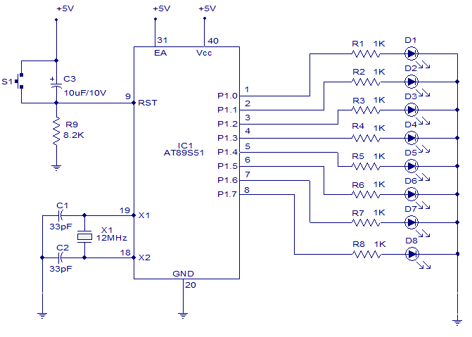
A six-function, eight-channel light chaser utilizing the 8051 microcontroller. The AT89S51, a member of the 8051 family, is employed to produce six distinct lighting sequences. The design incorporates straightforward software and hardware components. The circuit design features the AT89S51 microcontroller...
This circuit is designed to demonstrate high-frequency high voltage, capable of producing voltages up to approximately 30 kV, depending on the transformer used. It is economical and straightforward to construct, primarily utilizing a standard TV flyback transformer. The circuit...