
The basic circuit diagram of a constant current source mirror

The circuit operates as a current mirror, a fundamental configuration used in analog electronics to replicate a current in one branch of the circuit to another branch. In this design, transistors VT1 and VT2 are typically matched NPN or PNP devices, ensuring that they have similar characteristics, which is crucial for maintaining accuracy in current mirroring.
The circuit's operation begins with the reference current, which flows through VT1. This reference current is set by the resistor connected to the base of VT1. The output current, which is mirrored in VT2, is derived from the relationship established between the collector and base currents. The symmetry in the transistors ensures that variations in temperature or power supply do not significantly affect the performance of the current source.
In practical applications, this configuration is often used in differential amplifiers, current steering circuits, and biasing networks, where precise control of current is essential. The current mirror's ability to maintain a constant output current, regardless of load variations, makes it an invaluable component in integrated circuit design.
To enhance performance, additional components such as resistors or capacitors may be included to improve stability and bandwidth. Additionally, careful layout considerations are necessary to minimize parasitic capacitance and inductance, which can affect the circuit's performance. As shown for the mirror substantially constant current source circuit, wherein VT1, VT2 is matched to the tube. The figure shows Ir Ic2 + IB1 + IB2 Because VT1, VT2 are symmetr ical, their collector currents are equal to the base current, so there
Related Circuits
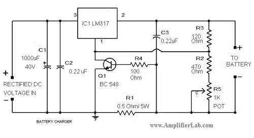
The circuit diagram of a lead-acid battery charger is presented here. The main component of this circuit is the IC LM317. The lead-acid battery charger circuit utilizing the LM317 voltage regulator is designed to efficiently charge lead-acid batteries while providing...

Phase noise is a critical performance parameter of frequency synthesizers for wireless applications. RF system designers of phase-modulated cellular systems, such as PHS, GSM, and IS-54, require low noise local oscillator (L.O.) or frequency synthesizer blocks. This document describes...
This signal generator is designed for the realignment of radio receivers. The unit is inexpensive and relatively simple but adequately serves its intended purpose. However, the output is not a pure sine wave, which may make it unsuitable for...

This simple mock flasher LED simulates the indicator of a sophisticated alarm system. It can be placed in doors, gates, and vehicles to confuse intruders. The mock flasher LED circuit is designed to mimic the flashing behavior of a typical...
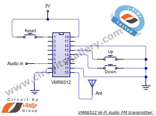
This article provides the circuit schematics for an FM transmitter along with the necessary explanations. The primary component utilized is the VMR6512 IC, a highly integrated FM audio signal transmitter chip designed for Hi-Fi audio applications. This chip can...
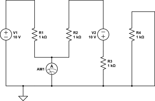
There is one significant low-impedance node in the entire circuit, referred to as 0V, located at the frame and the intersection in the middle. The upper voltage source is connected to this midpoint through a 1kΩ resistor, indicating that...