
Noise Floor Measurement Circuit of PLL Frequency Synthesizers

The phase-locked loop (PLL) circuit serves as a fundamental component in the design of frequency synthesizers, particularly for applications demanding precise frequency stability and low phase noise. The PLL architecture typically includes a high-stability crystal oscillator as a reference, which provides a stable frequency source. In this design, the 10 MHz crystal oscillator offers a reliable reference signal, ensuring minimal phase jitter, which is essential for maintaining signal integrity in RF communications.
The frequency synthesizer, exemplified by the National Semiconductor LMX2332TM, plays a crucial role in generating the desired output frequency while maintaining low phase noise characteristics. This device is capable of producing a range of frequencies with high precision, making it suitable for various RF applications. The inclusion of a voltage-controlled oscillator (VCO), specifically the ALPS URAE8x934, allows for dynamic frequency adjustment. The VCO's tuning constant of 27 MHz/V enables fine-tuning of the output frequency, which is phase locked to the 900 MHz target frequency.
The passive loop filter is designed to optimize the PLL's performance by shaping the loop response and ensuring stability across a range of frequencies. The choice of a relatively wide loop filter bandwidth of 15 kHz for a divide ratio of N = 4500 facilitates flexibility in adjusting the reference frequency without necessitating changes to the circuit components. This adaptability is critical for applications that may require varying frequencies under different operational conditions.
Phase noise measurements are a vital aspect of evaluating the performance of the PLL. By conducting measurements at a 150 Hz offset, the assessment focuses on the noise characteristics in the stable operating region of the PLL. The methodology of taking at least 20 video averages over a 1 kHz span enhances the accuracy of the phase noise data collected. Normalization of the spectrum analyzer measurements to dBc/Hz is essential for quantifying the phase noise floor, allowing for direct comparison against theoretical and practical benchmarks in RF design. The adjustment using 20 log N to reference noise to the phase detector input ensures that the final results accurately reflect the PLL's performance in terms of phase noise, which is critical for the reliability of wireless communication systems.Phase noise is a critical performance parameter of frequency synthesizers for wireless applications. RF system designers of phase modulated cellular systems, such as PHS, GSM and IS-54, need low noise local oscillator (L. O. ) or frequency synthesizer blocks. This is a design circuit for the measurement system. This is the figure of the circuit; The basic phase-lock-loop configuration we will be considering in the figure. The PLL consists of a high-stability crystal reference oscillator, a frequency synthesizer such as the National Semiconductor LMX2332TM, a voltage controlled oscillator (VCO), and a passive loop filter. The crystal reference used is the 10 MHz signal from the back of a spectrum analyzer at about +7 dBm or 1.
42 VPP. The VCO used for this test was an ALPS URAE8x934 VCO with a tuning constant of 27 MHz/V phase locked at 900 MHz. By using a relatively wide loop filter bandwidth, (15 kHz for N = 4500) we are able to vary the reference frequency from 30 kHz to 400 kHz without changing the component values and maintain loop stability.
The phase noise measurements were made at 150 Hz offset, to ensure that the data was on the flat portion of the curve inside the loop . At least 20 video averages were taken over a 1 kHz span for each measurement. In order to come up with the phase noise floor figure of merit the spectrum analyzer measurement must be normalized in terms of dBc/Hz, by subtracting 10 log of the resolution bandwidth used in the measurement.
The noise is then referenced to the input of the phase detector by subtracting 20 log N. 🔗 External reference
Related Circuits
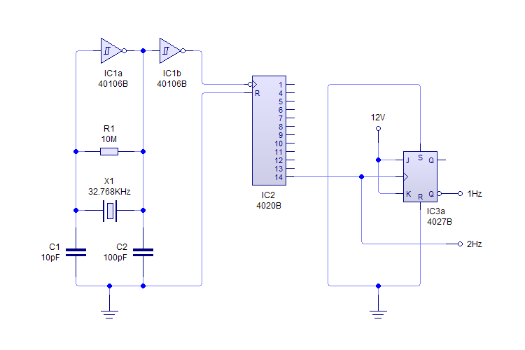
This plugin utilizes a quartz oscillator featuring a crystal (X1) to produce a 32,768 Hz (32,768 = 2^15) output. This frequency is fed into a 4020 14-Stage Ripple Counter, which divides the signal by 2^14, resulting in a 2...
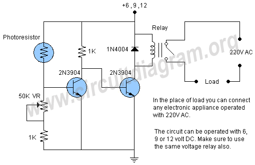
This project involves an automatic street light or lamp circuit designed to activate outdoor lights, such as garden lamps and night lights, automatically at sunset and turn them off at sunrise. The circuit is sensitive and versatile, capable of...
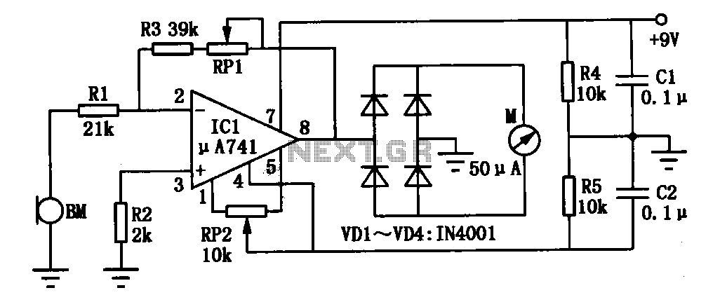
An environmental noise monitor circuit is presented. It primarily consists of a high-gain operational amplifier configured to amplify noise signals. The measured noise signal is displayed on an ammeter. The operational amplifier (IC1) receives the noise signal detected by...
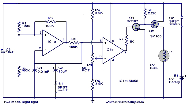
The operation and circuit diagram of a two-mode night light circuit are provided below. The two-mode night light circuit is designed to operate in two distinct lighting modes, typically offering a choice between a standard brightness setting and a dimmer,...
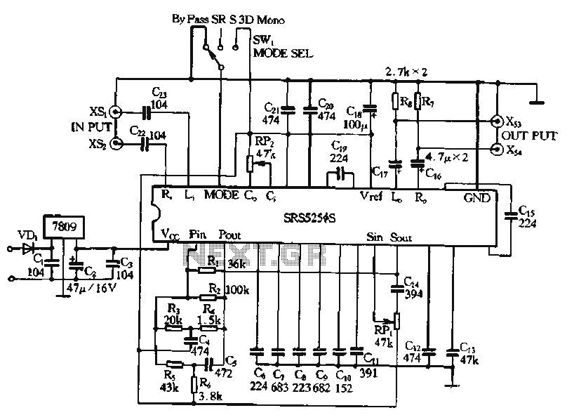
Typical application circuits for the Zheng brick SRS5250S are illustrated in the provided diagram. The SRS5250S features a pin diagram and a processing circuit that allows the user to switch between three operating modes: straight, SRS, and single-channel analog...
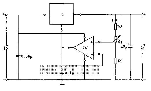
The circuit consists of resistors R1, R2, and RP, where the resistance values play a critical role in determining the magnitude of the current I. This current must exceed the input current of the operational amplifier, which is approximately...
Warning: include(partials/cookie-banner.php): Failed to open stream: Permission denied in /var/www/html/nextgr/view-circuit.php on line 713
Warning: include(): Failed opening 'partials/cookie-banner.php' for inclusion (include_path='.:/usr/share/php') in /var/www/html/nextgr/view-circuit.php on line 713