
The FSK signal demodulation circuit composed of the digital phase-lock
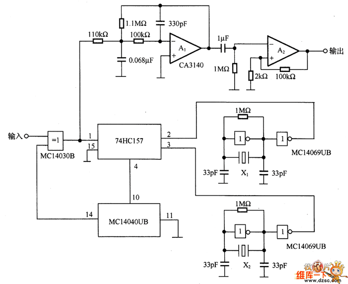
The FSK demodulation circuit is designed to recover the original data signal from an FSK-modulated carrier wave. The digital phase-locked loop (PLL) serves as the core component of the demodulation process, providing synchronization between the input signal and the local oscillator. The two crystal oscillators, X and X2, generate stable reference frequencies that are essential for accurate demodulation.
In this configuration, the crystal oscillator X operates at a lower frequency of 983.04 kHz, while the higher frequency oscillator X2 at 1.2288 MHz allows for the effective shifting of the carrier frequency. The 74HC157, a quad 2-input multiplexer, is utilized for frequency conversion, enabling the selection of the appropriate frequency for demodulation based on the input signal characteristics. The frequency splitting circuit further divides the output frequency to facilitate the processing of the FSK signal.
Overall, the combination of these components within the circuit ensures precise demodulation of the FSK signal, allowing for reliable data recovery. The design emphasizes stability and accuracy, making it suitable for various communication applications where FSK modulation is employed.In Figure 7-2 is the FSK signal demodulation circuit composed of the digital phase-lock. The circuit consists of 2 oscillators with different frequencies, i.e crystal oscillators X (the frequency is 983.04KHz) and X2 (the frequency is 1.2288MHz) compose the oscillator, and X2 consists of the frequency converting circuit 74HC157, frequency splitting circuit.. 🔗 External reference
Related Circuits
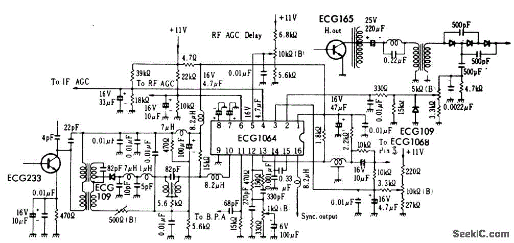
TV video signal processor circuit. The ECG1064 chip includes a primary video amplifier, two sync pulse amplifiers, a look-out protector, a noise detector, two noise gates, an automatic gain control (AGC) detector, an intermediate frequency (IF) AGC amplifier, a...
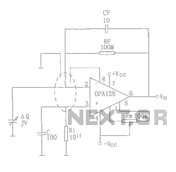
A charge amplifier is designed to amplify the signal charge from a piezoelectric device. It features a high internal impedance to accommodate the weak signal charge, which can be at the picoampere (pA) level. This necessitates a charge amplifier...
A substation capable of consuming 100 MVA with 375 kVA, 60 Hz input and 132 kV at 50 Hz using the same power. The challenge is to convert the 60 Hz input to 50 Hz, including a wiring diagram. To...
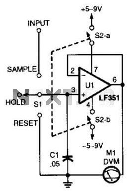
This circuit demonstrates the principle of the sample-and-hold circuit. SI can be replaced by electronic switches (FET, etc.) in an actual application. The sample-and-hold circuit is an essential component in various analog-to-digital conversion applications. Its primary function is to capture...
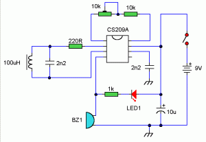
The core component of this DIY metal detector circuit is the CS209A. The metal detector is constructed with a single coil of 100 µH. The CS209A contains an oscillator that forms an LC circuit; the inductance of the coil...
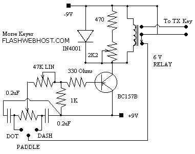
This is not a sophisticated automatic keyer but it is lot QRP to build and to have fun operating it. When the paddle is connected to the DOT terminal, C1 starts to charge. When C1's charge reaches sufficiently high value,...
Warning: include(partials/cookie-banner.php): Failed to open stream: Permission denied in /var/www/html/nextgr/view-circuit.php on line 713
Warning: include(): Failed opening 'partials/cookie-banner.php' for inclusion (include_path='.:/usr/share/php') in /var/www/html/nextgr/view-circuit.php on line 713