
The high-accuracy arbitrary waveform generator based on DDS is designed
DDFS and DDS represent a full digital method of waveform generation based on the sampling theorem. A DDS frequency synthesizer primarily consists of a phase accumulator, waveform data storage, a D/A converter, and a low-pass filter, as illustrated in the functional block diagrams. During each clock cycle, the phase accumulator adds the control word (representing frequency) to its current accumulated value, generating a new accumulated value. This value is then used as an address to read waveform data from the storage, which is subsequently sent to the D/A converter to convert the digital signal into an analog waveform, which is refined through a low-pass filter.
The periodic signal amplitude values are stored in the waveform data storage, and each overflow of the phase accumulator allows the reading of these amplitude values. If the frequency control word is designated as K and the phase accumulator has N locations, one clock cycle will result in the output of a periodic signal. The overall system clock rate is defined as fsclk, which determines the output signal frequency. The system block diagram is also provided.
The upper computer software is developed using LabWindows to generate control signals, while the lower-level unit uses an FPGA as its core to manage device operations. This unit is responsible for receiving control commands and signal parameters from the upper computer and coordinating the lower-level system to produce the desired waveform. The lower-level system comprises an FPGA control unit, waveform memory cell, and waveform production unit. The waveform memory cell includes FLASH and SRAM components. FLASH memory stores various waveform data, while during waveform generation, data is first read from FLASH into SRAM. The phase accumulator then retrieves this waveform data from SRAM.
The waveform production unit is responsible for generating the machine format of the waveform. It sends the waveform data read from SRAM to the D/A converter, creating a ladder array waveform, which is then output through a low-pass filter and power amplification circuit. The FLASH memory utilized is the U.S. semiconductor S29AL032D, with a capacity of 32 MB, designed to store various waveform data. As depicted in the relevant figure, specific address ranges within this memory store different types of waveform data, including sine wave, square wave, sawtooth wave, white noise, and user-defined data sections for four users.
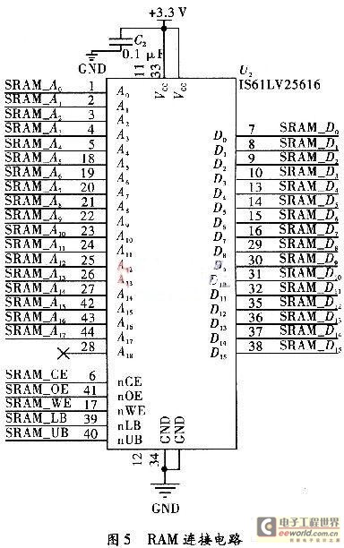
The RAM used is the IS61LV25616AL-10T, also from a U.S. semiconductor company, with a capacity of 256K x 16 bits, primarily for storing signal amplitude values during control commands and waveform generation.With the technical development, appearance and employing extensively of the large high-accuracy dynamic range D/ A converter at full speed of digital signal processing, because of sampling technique and computing technique, generated frequency is relatively fixed with the phase place through the digital means and adjustable synthetic technology, n amely DDFS DDS Technology is ripe day by day, it adopts the structure of Full Digitalization, it is fast to have high, relative bandwidth wide, frequency conversion of frequency resolutioning, the phase noise is low, higher advantage of signal purity. So, this system finishes the arbitrary waveform generator to design by DDS technology. DDFS DDS Technology is an undulate generation method of Full Digitalization based on sampling theorem.
DDS frequency synthesizer mainly made up of phase place accumulator, undulate data storage, D/ A converter and low-pass filter, their functional block diagrams are shown as in Fig. 1. Within a systematic clock cycle, accumulator primary accumulated value and control word of the frequency of phase place are added, receive the new accumulated value, regard new accumulated value as the address, read the range value of the signal from the undulate data storage, send into D/ A converter and change the digital signal into the analog signal, is turned into and needs the waveform by the low-pass filter afterwards.
Among them has stored the single periodic range value of the periodic signal in the undulate data storage, the phase place accumulator overflows once each time, can read a periodic signal amplitude value from the undulate data storage. So, if suppose the control word of the frequency is K, the phase place accumulator is N location, passes a clock cycle systematically, can produce a periodic outcoming signal, and then set systematic clock rate as fsclk, output the signal frequency.
The overall block diagram of system is shown as in Fig. 2. Among them, the software of upper computer is written by LabWindows software, for the production of the control signal, the lower-position unit regards FPGA as the core and controls the device, is used mainly for receiving control command and signal parameter that the upper computer sends, and control the lower-position unit system to produce and correspond to the waveform. The lower-position unit system is mainly divided into FPGA control unit, undulate memory cell, wave form and produced the unit.
Undulate memory cell mainly includes FLASH and SRAM, FLASH is used for storing various undulate data, when the waveform is produced, the undulate data that FPGA will be produced first read in SRAM from FLASH, the accumulated value which reuses the phase place accumulator reads the undulate data from SRAM. The waveform produces the unit and mainly finishes the machine format production of the waveform, send the undulate range data that SRAM read out into D/ A converter at first, produce the ladder array wave of the signal, and then produce the outcoming signal through the low-pass filter and amplifying circuit of power.
FLASH adopt U. S. A. fly to, ask for semi-conductive S29AL032D of Company, its capacity is 32 MB, it is used for storing various corrugate range information, it stores the form and is shown as in Fig. 4. Knowing by Fig. 4, the address section 0G—000000- 0x01FFFF stores sine wave range value, address section 0G—020000-0x03FFFF stores the chopping sea data, the address section 0G—040000- 0x05FFFF stores the sawtooth wave data, address section 0G—060000-0x07FFFF stores the white noise data, 0G—080000- 0x0FFFFF among the address areas is the self-defining districts of 4 users, store the cycle that 4 kinds of users need to produce undulate data.
RAM adopts the American core IS61LV25616AL-10T of the semi-conductive department, its capacity is 256* 103* 16 Bit, is used mainly for storing the range value of the signal when control command and wavefor 🔗 External reference
Related Circuits
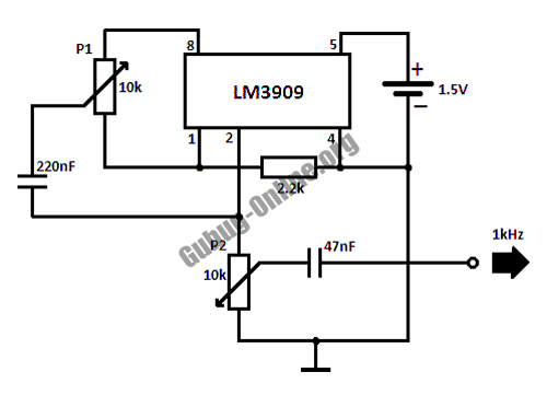
This circuit design for a high-frequency waveform generator is highly beneficial for electronic experiments and designs. The circuit generates sine wave oscillations, but it can also be modified to produce triangle or square wave functions. The high-frequency waveform generator circuit...
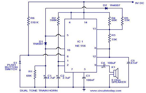
A dual-tone model train horn/sound generator/simulator circuit can be created using two NE 555 timers connected in cascade. However, the circuit diagram presented is designed with the NE 556 integrated circuit, which essentially comprises two 555 timers in a...
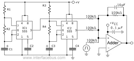
This circuit combines the outputs from two distinct 555 multivibrators using a summing operational amplifier (Op Amp). It serves to illustrate an alternative implementation of a 555 timer, with most background calculations addressed in other sections. The standard configuration...
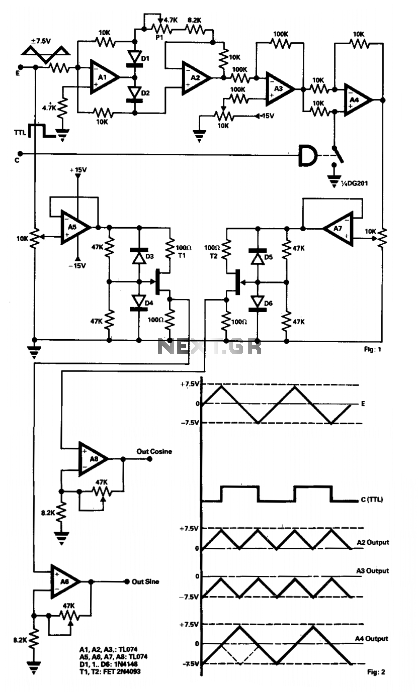
The presented circuit generates waveforms from any function generator that produces a triangular output and a synchronized TTL square wave. Amplifiers A1 and A2 function as a two-phase current rectifier by inverting the negative voltage at the input of...
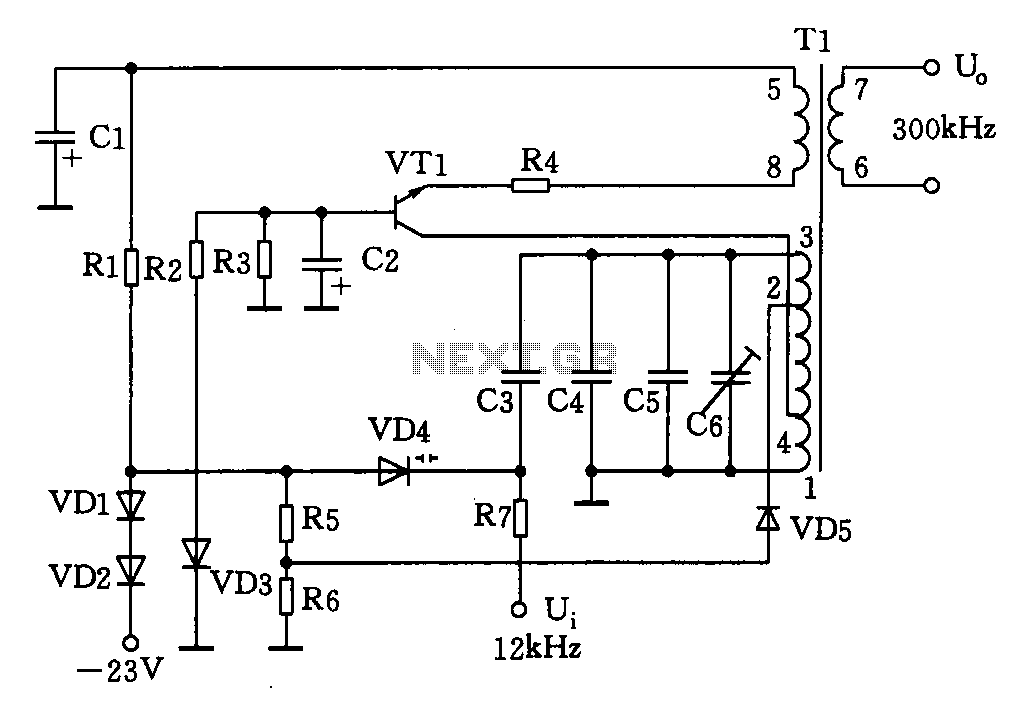
This circuit is designed for a 300 kHz signal generator. It includes components such as VT1, T1, VD4, and other associated elements. The voltage-controlled oscillator (VCO) employs an LC-tuned collector, with VT1 functioning as the oscillating transistor, varactor diode...
This regulator is designed to control a DC generator. In this configuration, one side of the field is grounded. Diode D4 prevents the battery from discharging through the generator and serves as a replacement for the mechanical cut-out relay....