
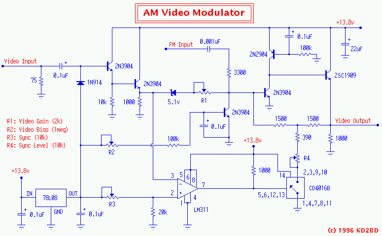
The KD2BD ATV AM Video Modulator
When the Brookdale ATV Repeater System was first constructed, a PC Electronics model RTX-70 exciter was used in the transmitter portion of the repeater. However, the intermodulation distortion products generated by the exciter when amplified by a Mirage D100ATV-R amplifier were so severe, they completely overwhelmed the repeater's receiver, despite the extensive combline and interdigital filtering used in the system.
After much study and research, the cause of the exciter's strong IMD products was found to be the result of distortion and non-linearity in the exciter's video modulator, and not the modulated RF stages themselves. Once the original video modulator was replaced with the one described on this page, the harmful effects of IMD were reduced to imperceptible levels. An added bonus was a noticeable increase in the exciter's RF power output. This method of sync expansion is unique in that it also compensates for audio subcarrier compression at sync time, resulting in a clean output signal with no sync buzz in the transmitted audio. The first section of the video modulator performs a video level clamping function. The high input impedance Darlington amplifier and the small series coupling capacitor combine to achieve an excellent low-frequency response and a clamping function with very rapid response time. A three terminal voltage regulator sets the clamping level to 8 volts. The clamped video is then level shifted through a zener diode and applied to a single video amplifier stage. A PNP transistor in the collector circuit functions as a constant current source for the video amplifier. The use of a constant current source rather than a collector load resistor in the video amplifier results in very high voltage gain with nearly rail-to-rail output voltage capability. Negative feedback around the video amplifier reduces the gain to the amount required, while it increases the bandwidth, flattens the frequency response, increases the linearity, and reduces any distortion products to extremely low levels.
The described circuit utilizes a 2N3904 transistor to establish the quiescent point (Q point) for the amplifier, which is crucial for linear amplification. The inclusion of a 3300-ohm resistor and a DC blocking capacitor allows for the integration of FM subcarrier audio at 4.5 MHz into the base circuit, ensuring that the audio signal is properly coupled without DC offset affecting subsequent stages. The RF power stage employs a 2SC1909 transistor, noted for its capability to handle high frequencies and power levels, making it suitable for the final amplification stage of the modulator.
In addition, the circuit includes an LM311 voltage comparator that processes clamped video signals for sync detection. The option to use an LM1881 sync separator chip provides flexibility in design, catering to varying builder preferences. The output sync pulses trigger a CD4016B silicon bilateral switch, which dynamically adjusts the negative feedback around the video amplifier. This adjustment is critical during sync periods, as it mitigates the effects of gain compression that may occur in linear power amplifiers following the video modulated stages.
The design of the video modulator emphasizes the importance of maintaining a clean output spectrum, particularly in the context of an ATV repeater system. The original use of a PC Electronics RTX-70 exciter highlighted the challenges posed by intermodulation distortion (IMD), which can severely impact system performance. By replacing the initial video modulator with a more efficient design, significant improvements in both RF output and reduction of IMD were achieved.
The implementation of a high input impedance Darlington amplifier combined with a fast-acting clamping capacitor allows for rapid response to video signals, ensuring that the signal integrity is preserved. The voltage regulator, set to 8 volts, establishes a stable clamping level, while the subsequent level shifting through a zener diode prepares the signal for amplification.
The video amplifier stage benefits from a constant current source configuration, enhancing voltage gain and enabling nearly rail-to-rail output. This approach, coupled with negative feedback, optimizes performance by broadening bandwidth, improving frequency response, and minimizing distortion, thus ensuring high fidelity in the transmitted video signal.A 2N3904 in the base circuit sets the `Q' point of the amplifier. FM subcarrier audio at 4.5 MHz is also injected at this point through a 3300 ohm resistor and a DC blocking capacitor. A high frequency 5-watt RF power transistor (2SC1909) serves as the last stage of the modulator. An NTE-235, NTE-236, or equivalent is suitable in this application. Clamped video is also fed into an LM311 voltage comparator that serves as a video sync detector. Some builders have used an LM1881 sync separator chip for this stage. Either way, sync pulses detected by this circuit trigger a CD4016B silicon bilateral switch that lowers the negative feedback around the video amplifier and voltage follower at sync time to compensate for high power gain compression in any solid-state linear power amplifiers that may follow the video modulated stages.
Building an in-band, duplexed ATV repeater system is not a trivial task. Just ask anyone who's tried. The output spectrum of the repeater's transmitter must be extremely clean, and both the transmitter's output as well as the receiver's input must be tightly filtered to achieve adequate isolation and reject interference from strong signals on neighboring frequencies. When the Brookdale ATV Repeater System was first constructed, a PC Electronics model RTX-70 exciter was used in the transmitter portion of the repeater.
However, the intermodulation distortion products generated by the exciter when amplified by a Mirage D100ATV-R amplifier were so severe, they completely overwhelmed the repeater's receiver, despite the extensive combline and interdigital filtering used in the system. After much study and research, the cause of the exciter's strong IMD products was found to be the result of distortion and non-linearity in the exciter's video modulator, and not the modulated RF stages themselves.
Once the original video modulator was replaced with the one described on this page, the harmful effects of IMD were reduced to imperceptible levels. An added bonus was a noticeable increase in the exciter's RF power output. This method of sync expansion is unique in that it also compensates for audio subcarrier compression at sync time, resulting in a clean output signal with no sync buzz in the transmitted audio.
The first section of the video modulator performs a video level clamping function. The high input impedance Darlington amplifier and the small series coupling capacitor combine to achieve an excellent low-frequency response and a clamping function with very rapid response time. A three terminal voltage regulator sets the clamping level to 8 volts. The clamped video is then level shifted through a zener diode and applied to a single video amplifier stage.
A PNP transistor in the collector circuit functions as a constant current source for the video amplifier. The use of a constant current source rather than a collector load resistor in the video amplifier results in very high voltage gain with nearly rail-to-rail output voltage capability.
Negative feedback around the video amplifier reduces the gain to the amount required, while it increases the bandwidth, flattens the frequency response, increases the linearity, and reduces any distortion products to extremely low levels. 🔗 External reference
Related Circuits
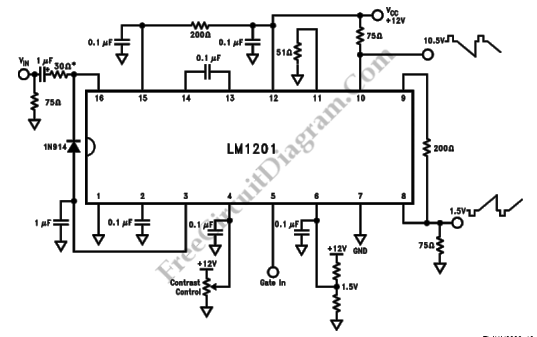
This is a schematic diagram of a video amplifier circuit with bi-phase output. The bi-phase output generates both positive-going and negative-going signals, enabling balanced signaling. The primary component of this circuit is the LM1201. In this configuration, the inverted...
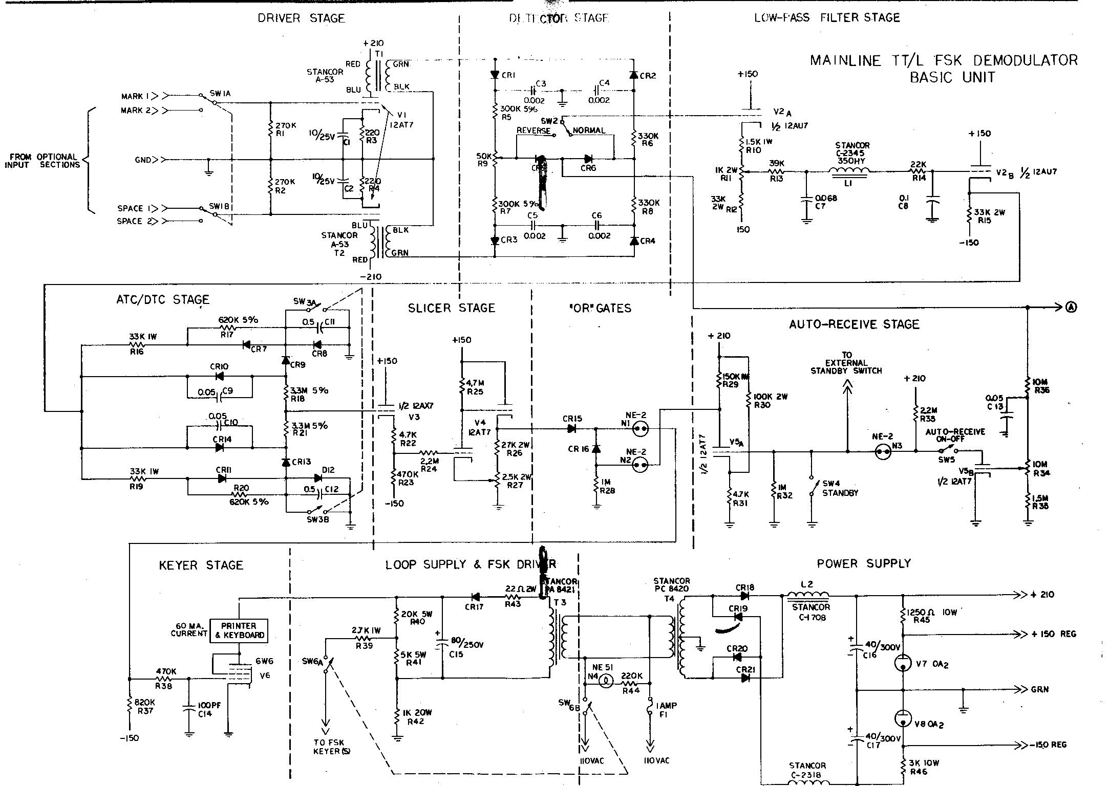
The term "demodulator" is becoming a standard in both commercial and military sectors. "Converters" are often associated with devices that automatically transform Morse code into RTTY, convert 8-level signals to 5-level, or adjust baud rates from 50 to 45,...
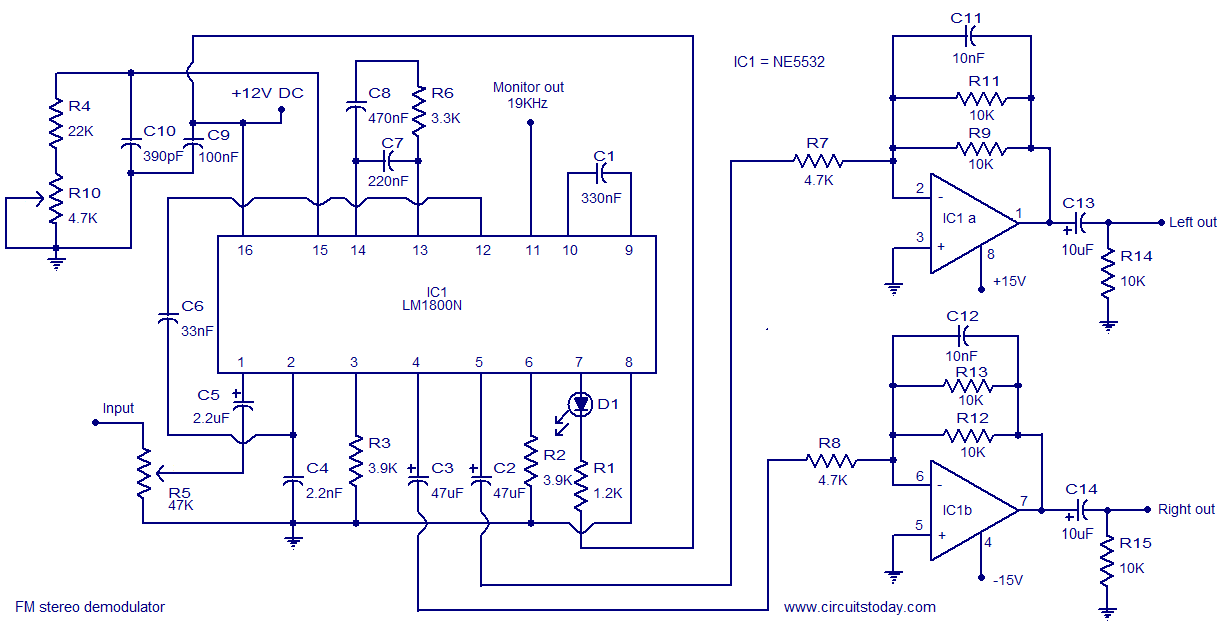
The following circuit illustrates the LM1800 IC Integrated FM Stereo Demodulator Circuit. Features include excellent sound quality and high-quality FM stereo. The LM1800 Integrated Circuit (IC) serves as a highly effective FM stereo demodulator, designed to deliver superior audio performance...
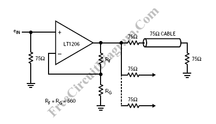
The LT1206 is designed to drive multiple video cables, featuring a bandwidth of 60 MHz, an output current capability of 250 mA, and low output impedance. The LT1206 operational amplifier is optimized for video signal applications, making it an excellent...
The TBA120 Series integrated circuits (ICs) offer a high-gain limiting intermediate frequency (IF) amplifier and a quadrature coincidence detector in a single package. These ICs are primarily designed for the extraction of television intercarrier sound, which is frequency modulated...
There have been numerous discussions regarding the Lilliput's inability to automatically switch, despite the presence of this feature in the secret menu. The Lilliput display is a versatile device often used in various applications, including professional video production and...
Warning: include(partials/cookie-banner.php): Failed to open stream: Permission denied in /var/www/html/nextgr/view-circuit.php on line 713
Warning: include(): Failed opening 'partials/cookie-banner.php' for inclusion (include_path='.:/usr/share/php') in /var/www/html/nextgr/view-circuit.php on line 713