
The many DC to DC converters using IC-555

The circuit operates as a versatile voltage doubler, effectively transforming a lower voltage DC input into a higher voltage output, suitable for various electronic applications. The NE555 timer IC serves as the core component, functioning as an astable multivibrator to generate a square wave signal that drives the voltage doubling mechanism. The arrangement of components allows for efficient voltage conversion, with the rectification and filtering stages ensuring a stable and smooth DC output. The design can be adapted for different input and output voltage requirements, demonstrating flexibility in its application. This circuit is ideal for powering low-current devices where a higher voltage is necessary, offering a reliable solution for electronic projects and applications.This be Simple Doubler Voltage circuit, from voltage 12VDC to be 24VDC. By use Timer IC highly popular the number NE555 and other equipment a little again. It can give current get about 50mA convenient for the circuit, that use low current the small-sized. The principle works of the circuit be, When use Volt input 12VDC give with the circuit will touch Filter current smoothly with increasingly. The capacitors C5 give with IC1, The resistor R1, R2 and, capacitors C1, Which build the circuit model astable multi vibrator Square wave generator, at the frequency about 2KHz come out the way pin 3 of IC1. By have capacitors C3, C4 diode D1 and D2. Which build be boost up voltage x 2, which will enhance the level Volt out be the direct current about 24VDC or 2 times of the level Volt input.
This circuit is called DC TO DC converter circuit. Which increase the voltage circuit. There can be customized to change the output values. For example 6Vdc to 12Vdc, 12Vdc input to 24Vdc output. When the power supply input to IC1-NE555 is the output pin 3 at a frequency of 1 kHz. The frequency is Q1-BC547 and Q2-BC557, which will continue to use push pool work interchangeably. If this is the positive output signal Q1 Q2 will run the delete function this reason, C2 and C3 capacitors are half-wave alternating. To test the circuit or circuits that may need some circuits, but we have no fire-5V power supply-5V, but if the battery 9V circuit can allow us to use the volt-5V as desired.
By using IC NE555, which causes wave square the sector output allows the voltage about 6V when the signal on the output from a pulse plus C2 acts charge through D1 to ground and if the pulse negative capacitor C2 will discharge. through diode D1 and capacitor C3 to chage that negative voltage is about-6V, but being removed to the number of left-5V zener diode ZD1 current output will be approximately 12mA.
Work of the circuit is IC1, R1, R2 and C1. The range of the A Stable Multi Vibrator, and the output is a square wave. It is a positive signal pulse frequency of 2. 3 kHz output pin 3 of IC1. And C3 and D1 connected to circuit CLAMP. That it serves to signal a positive pulse to pulse signal negative. The D2 and C3 act negative pulse signal is converted direct current (DCV) electrical signals. The negative power. Thus the output voltage to a negative DC electrical. This circuit is used IC number NE555 set up to stable multi vibrator. It produces a frequency rectangular patch of about 100 Hz. Out to pin 3 through C3 and C4. Before the rectifier power section. Both positive and negative DC 2 series. Positive power supply will work with the rectifier D1 and D2. When a positive signal to be via D2 to the output. And filtered from C5 to filter the pressure to smooth again. But if there is negative signal to the D1 and down through the ground. The negative power of the D3 and D4 the rectifier. When a negative signal to the output signal to be via D3. And will be filtered from C6 to smooth again. When a positive signal to be via a D4 to ground. 🔗 External reference
Related Circuits
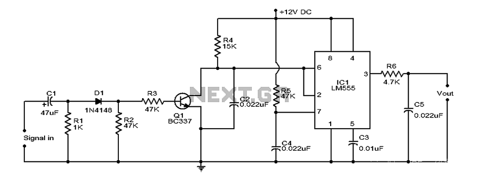
This document provides an overview of a simple circuit diagram for frequency (F and V) voltage conversion. It describes a digital frequency meter circuit primarily based on the LM555 timer IC, which is commonly used in various applications, including...
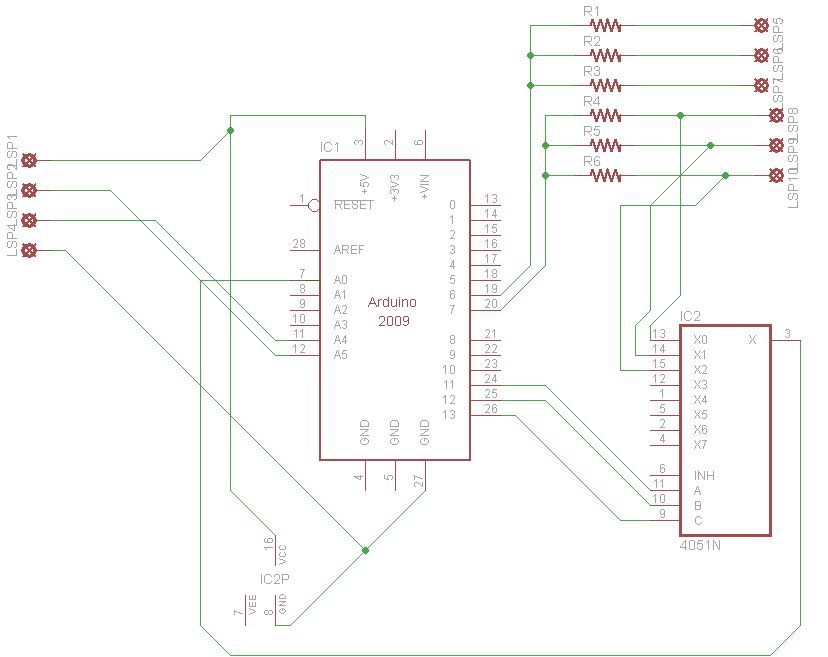
This guide explains how to set up an automated gardening system using an Arduino and other inexpensive electronic components. The system promotes sustainable gardening by utilizing sensors to measure soil moisture and a web scraper to forecast future weather...
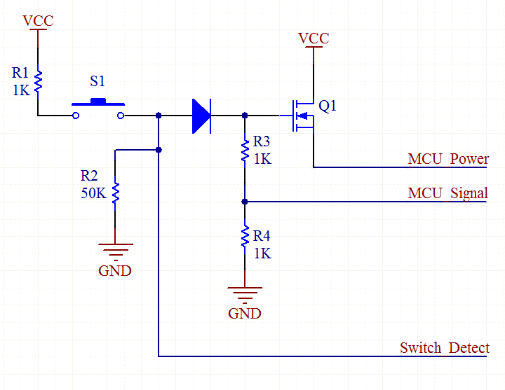
An explanation of how the circuit operates. The TPS_EN line is initially low, as it is connected to a 10k pull-down resistor (not shown in the schematic). When the user presses switch S2, the MOSFET Q2 is activated because...

By adding the same circuit in parallel, the number of inputs can be increased according to the applications. Each input is connected to the inverting terminal of the LM3900. The built-in amplifier of each section amplifies every audio input...
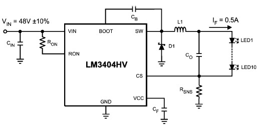
The LM3404 is a monolithic switching regulator that can be utilized to design a simple constant current driver for high-power LEDs. This LED driver project is suitable for automotive, industrial, and general lighting applications. Hysteretic control of the on-time,...

This article describes a 2-Input alarm developed on the PIC LICK-1 Module using a Microchip PIC16F628-04. The program uses the internal 4MHz oscillator and if any other frequency is used, the timer values will need to be changed. A...