
Conversion using LM555 timer circuit diagram
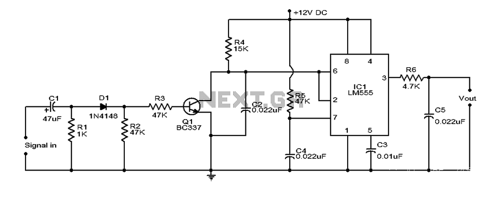
The circuit described utilizes the LM555 timer IC, which is versatile and widely used in timing applications. In this configuration, the LM555 is set up in monostable mode, where it generates a single output pulse in response to a trigger signal. The width of this pulse is determined by the values of resistor R4 and capacitor C2, which create a timing interval that corresponds to the frequency of the input signal.
The inclusion of transistor T1 is critical for the operation of the circuit. It acts as a switch that allows for the rapid discharge of capacitor C2, enabling the LM555 to be re-triggered effectively. This ensures that the output pulse width is consistent and accurately reflects the input frequency.
Capacitor C1 plays a vital role in isolating the DC component of the input signal. This isolation is essential for preventing any DC offset from affecting the timing characteristics of the LM555. Proper assembly of the circuit board is crucial, and it is recommended to perform this in a clean and controlled environment to avoid any interference or damage to the components.
The circuit requires a stable 12V DC power supply to operate effectively. It is important to note that the output is a PWM waveform rather than a pure DC signal. Therefore, if a pure DC output is desired, additional circuitry, such as a low-pass filter or a dedicated DC converter, must be implemented to process the PWM signal accordingly.
In summary, this circuit diagram serves as a foundational design for frequency-to-voltage conversion applications, leveraging the capabilities of the LM555 timer IC and additional components to achieve the desired output. Proper implementation and additional filtering are necessary to ensure the output meets the specific requirements of the application.Explanation Here is a simple circuit diagram frequency (F and V) voltage conversion. It found that the digital frequency meter circuit, the circuit is mainly based on a LM555 t imer IC tachometer and other projects in the large number of applications. The IC is wired shooting mode to the mono a fixed pulse width, PWM frequency of the input signal of variable frequency. Resistor R4 and capacitor C2 provide the necessary timing circuitry. In the form of transistor T1 parallel to the C2 discharge path it is necessary to re-trigger the IC. Capacitor C1 as the input DC isolator. Schematic Precautions The circuit board assembly in Verona. A 12V DC power supply circuit. LM555 must be installed in the holder. The output of this circuit is not a pure DC, but the PWM waveform. Additional circuits require pure DC converter PWM waveform.
Related Circuits
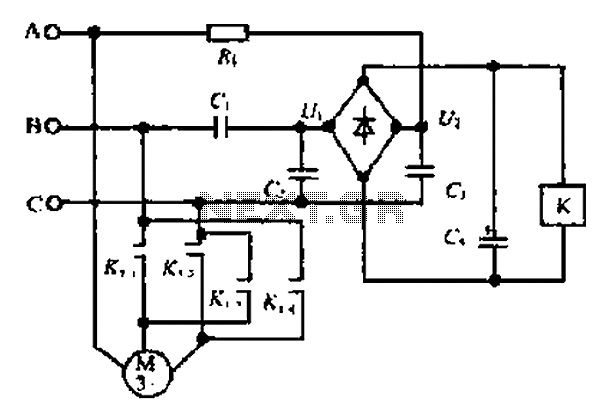
Composition ratio circuit. The circuit consists of resistors and capacitors that form a shift register circuit with diodes VD1 to VD4, creating a bridge for electric current. Capacitor C4 is utilized for filtering applications and for eliminating instantaneous relay...
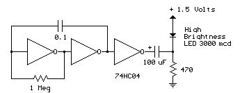
Several 1.5 V LED flasher circuits can be found online, and four of them are presented here. The flasher circuits operate on a single 1.5 V power supply. The design of a 1.5 V LED flasher circuit typically involves a...

The circuit has four inputs. The voltage gain between each input and the output is maintained at unity by the relative values of the 470 kΩ input resistor and the 470 kΩ feedback resistor. The described circuit operates as a...
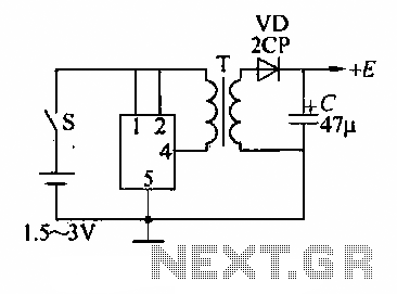
A DC booster circuit is illustrated in the figure, which represents a step-up transformer circuit diagram. The step-up transformer (T) can be utilized to power small transistor radios. The winding ratio can be adjusted to achieve the desired output...
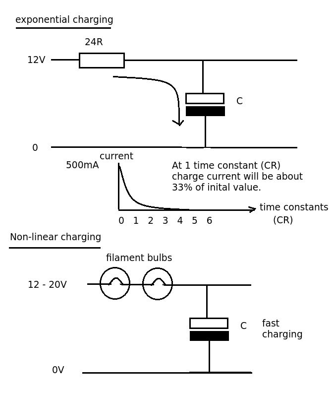
Designing a simple current limiter that charges a large 4.7mF capacitor with a charge current of approximately 500mA from a supply voltage of 10-20V. The dilemma is that there are existing MMBT2222A transistors available, which would be preferable to...

Most consumer electronic devices utilize infrared remote controls for convenient operation. The carrier frequency of these remote controls typically ranges from 36 kHz to 38 kHz. Control codes are transmitted to the device's receiver in a serial format, which...
Warning: include(partials/cookie-banner.php): Failed to open stream: Permission denied in /var/www/html/nextgr/view-circuit.php on line 713
Warning: include(): Failed opening 'partials/cookie-banner.php' for inclusion (include_path='.:/usr/share/php') in /var/www/html/nextgr/view-circuit.php on line 713