
The Measurements for MIT 3DL1 Run
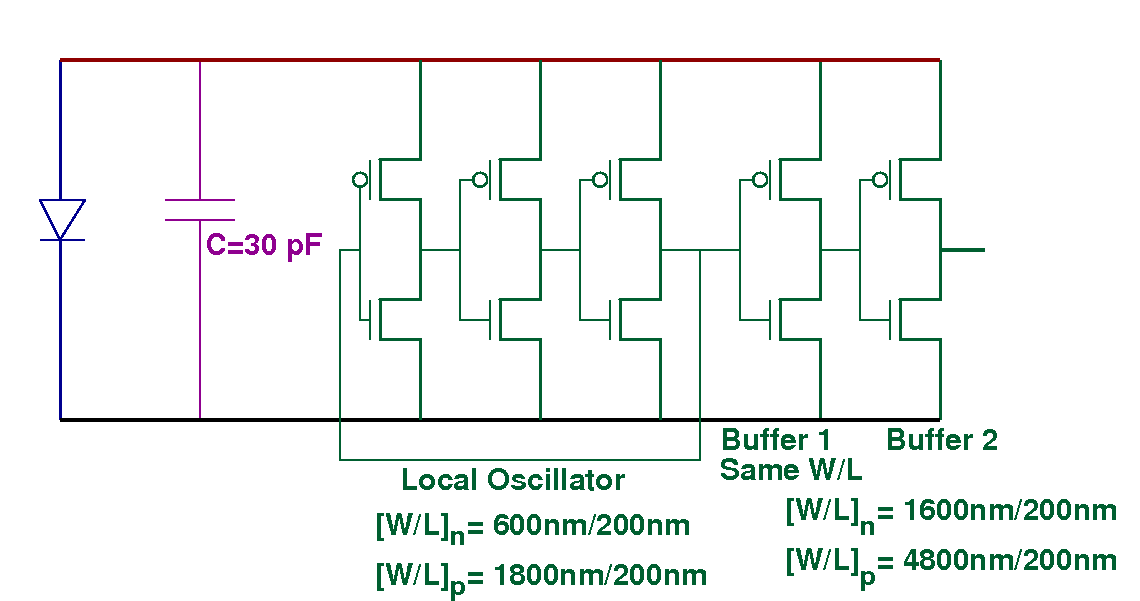
The described circuit involves photodiodes that are responsive to various light sources, including laser pointers, LED lights, sunlight, and fluorescent lighting. The performance metrics indicate that the photodiodes exhibit a significant voltage output, which varies according to the intensity and type of light source. The observation of 300 mV under a laser pointer suggests a high level of sensitivity and efficiency in converting light energy into electrical energy, particularly under focused light conditions. The lower outputs under LED and fluorescent lighting indicate a reduced sensitivity or lower intensity of these light sources compared to the laser.
The simulation results predicting DC rail voltages of around 300 mV under red light at 1 kW/m² suggest that the photodiodes are designed to operate effectively in high-intensity environments, potentially making them suitable for applications requiring precise light detection. The noted intensity of 333 W/m² from the laser pointer indicates that the photodiodes are capable of handling high power levels without saturation, which is critical for accurate measurements in varying lighting conditions.
The phenomenon of increased current generation, attributed to multiple absorptions and reflections within the photodiode structure, highlights the importance of the design of the diode layers and their arrangement. The interaction of light with the different tiers of diodes and the reflective properties of the underlying metal layers can enhance the overall efficiency of the photodiodes, making this configuration advantageous for applications in optical sensing and detection systems. The insights gained from these observations can inform future designs and improvements in photodiode technology, particularly in optimizing their performance across a range of illumination conditions.The chips that are termed "working well" yield about 300 mV under the beam from a laser pointer and between 40 to 80 mV under the LED light. Voltages around 100 mV were observed in a sunlit room and about 10 mV under fluorescent lighting. Our simulations ( see the design report in PDF ) predicted DC rail voltages of around 300 mV under 1 KW/m2 red light.
The laser pointer power isn`t specified beyond it is "< 5 mW"; estimating its beam size to be about 15 mm2 at the distance from which we have usually used it on the chip, the highest possible intensity the chip receives is around 333 W/m2. This result seems to indicate that the photodiodes are generating more current than was calculated; the disparity is probably due to multiple absorptions as the beam passes through the top tier of diodes and is reflected back from the metal layers of the tiers underneath.
🔗 External reference
Related Circuits
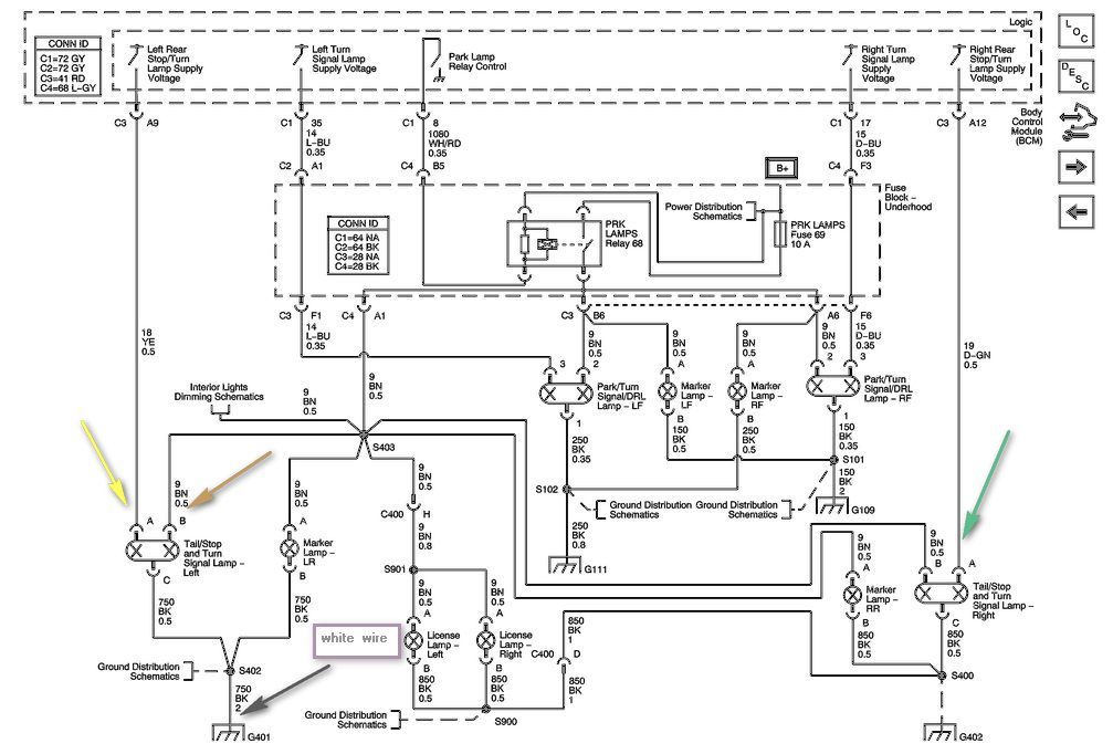
The left side of the vehicle operates correctly, with the running lights and brake light functioning properly. However, the turn signal is not working when wired directly into the harness. There is a preference to avoid purchasing a plug-in...
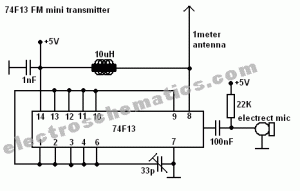
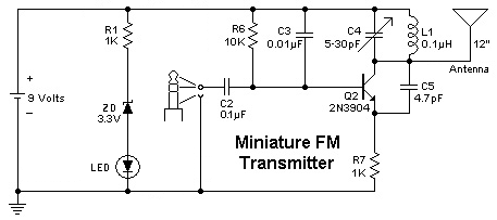
This FM spy transmitter can function as a bug transmitter or a DIY FM bug. It utilizes a single IC 74F13, one coil, a capacitor, and one additional component. The FM spy transmitter is a compact device designed for covert...
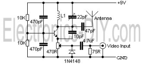
The video transmissions from this unit can be received on a small portable, tunable, and battery-operated TV set, similar to those found in flea markets. The described unit is capable of transmitting video signals that can be captured by compact,...
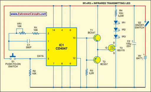
Most IR remotes operate reliably within a range of 5 meters. The complexity of the circuit increases when designing an IR transmitter for reliable operation over a longer range, such as 10 meters. To double the range from 5...
To replace a microphone with a 3.5" audio jack in a circuit, modifications will be necessary. The circuit currently utilizes an electret microphone, and adjustments must be made to accommodate the audio jack for audio transmission. The audio jack...
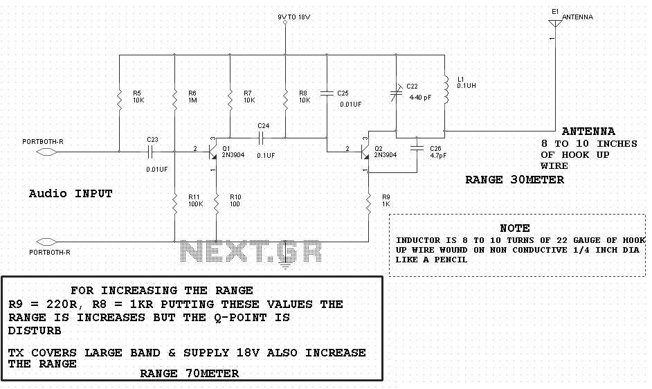
An FM and AM transmitter integrated into a compact device utilizing the CD4001 integrated circuit. It broadcasts at 20 MHz for AM and 100 MHz for FM. The described transmitter combines both Frequency Modulation (FM) and Amplitude Modulation (AM) capabilities...