
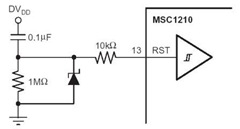
The MSC1210 Typical External Reset Circuit Schematic
The flash memory schematic involving the MSC1210 microcontroller incorporates several critical reset mechanisms that ensure reliable operation across various scenarios. The power-on reset provides an initial state for the device when power is applied, while the external reset allows for manual or external control over the device's state. Software reset can be triggered through specific instructions in the code, enabling the program to recover from errors or to restart processes without physical intervention.
The watchdog timer reset serves as a fail-safe mechanism, resetting the device if it becomes unresponsive due to software malfunctions. The brownout reset protects the device from operating under insufficient voltage conditions, which could lead to unpredictable behavior.
The recommended external reset circuit for the MSC1210, featuring a 10 kΩ resistor, is designed to ensure that the RST pin is adequately pulled high during the reset process. This resistor value is optimal for balancing the response time and power consumption of the circuit. When the RST pin is driven high for two tOSC periods, it effectively halts all operations, ensuring that the microcontroller is in a safe state before executing a reset. After this period, pulling the RST pin low initiates the reset sequence, allowing the device to resume normal operation.
In summary, this flash memory schematic provides a robust framework for managing various reset conditions in the MSC1210 microcontroller, ensuring reliable performance and stability in electronic applications.and Flash Memory schematic that can be done from the following sources: power-on reset, external reset, software reset, watchdog timer reset, and brownout reset. The figure (click to enlarge) shows a recommended external reset circuit for the MSC1210 with the serial 10kOhm resistor recomendation for any configuration of this reset type.
According t othe MSC1210 datasheet, you willperform an external resetby taking RST pin high for two tOSC periods as this stops device operation, crystal oscillation, causes all digitall pins to be pulled high from that point and then followed by taking the RST pin low that initiates the reset procedure. 🔗 External reference
Related Circuits
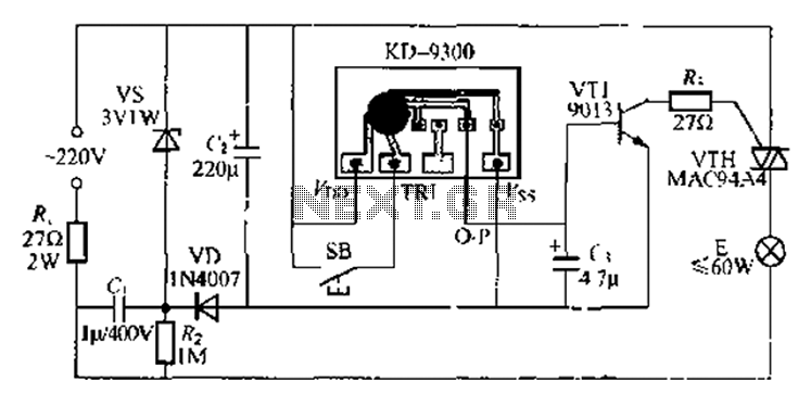
The circuit utilizes a KD-9300 music IC, which activates when the button switch (SB) is pressed, causing the electric lamp (E) to light up for approximately 20 seconds before automatically turning off. The setup includes a half-wave rectifier and...
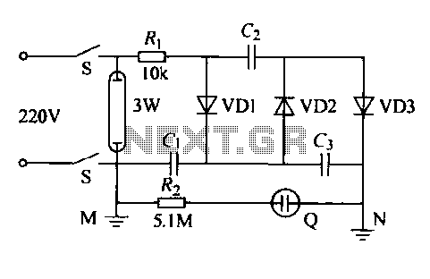
The IED functions as a hotel, restaurant, and family-oriented tool designed for the effective eradication of mosquitoes, as illustrated in Figure 16-12a. It employs a diode voltage doubler rectifier circuit to generate a high voltage. When mosquitoes are attracted...
When running large-scale software or games, a computer's internal temperature can increase significantly, especially during hot summer months. Although the machine is equipped with a CPU and graphics card fan, poor hot air circulation prevents immediate removal of heat...
The aboriginal accessory forms a typical oscillator circuit that produces both a triangle waveform signal and a square wave signal. The triangle signal is fed into a voltage regulator circuit, which converts the triangle voltage signal to a triangle...
The transmitter features a VXO circuit that drives a keyed amplifier. This keyed amplifier powers an MRF 476 final amplifier, producing approximately 2 watts of output. Additionally, a solid-state T-R switch is incorporated for the receiver. The component values...
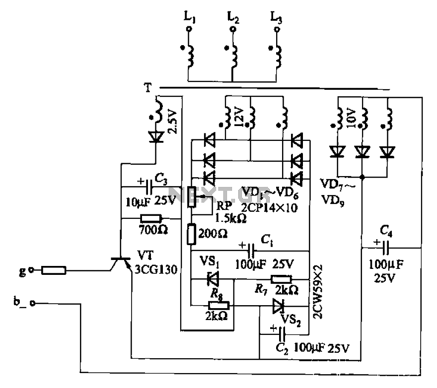
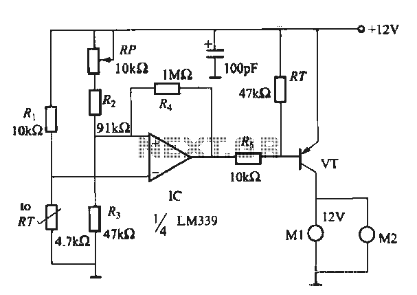
The CJ-12 Excitation Regulator is designed for automatic excitation control of small generators with a capacity of 250 kW or less. Its circuit is illustrated in Figure 7-45. The adjustment potentiometer RP allows for the modification of the measuring...