
THE ZX97LITE SCHEMATIC
The ZX97Lite is designed as a compact and efficient alternative to the original ZX97, making it more accessible for hobbyists and engineers alike. Its single-sided PCB layout significantly reduces manufacturing complexity and costs, allowing for easier replication and modification. The omission of certain components, such as the RAMdisk and the 8255 parallel port, streamlines the design while still retaining the essential functionalities of the ZX81.
The architecture of the ZX97Lite emphasizes modularity, with the circuit divided into smaller functional subsystems. This modularity not only simplifies troubleshooting and upgrades but also enhances educational opportunities for those interested in understanding the workings of retro computing systems. The choice of the Z80 CPU, a well-documented and widely supported microprocessor, ensures that developers have access to a wealth of resources for programming and interfacing.
The power consumption of 50mA is particularly advantageous for portable applications, enabling the use of batteries or solar cells, which aligns with modern trends toward sustainable technology. The bank-switched RAM/EPROM disk feature allows for flexible software management, catering to the needs of users who may wish to run multiple programs or applications without requiring extensive hardware modifications.
In summary, the ZX97Lite represents a significant advancement over its predecessor while maintaining compatibility with the ZX81, making it a valuable addition to the lineage of personal computing. Its thoughtful design and user-friendly features ensure that it remains relevant in the current landscape of electronics and computing.I designed the ZX97 as a discrete copy of the ZX81, which was the first PC for millions of people. In the process ZX97 turned into much more than a mere copy. While it is backward compatible with the ZX81, it is in all other respects a significant improvement over the ZX81. In 1998, Rodney Knaap contacted me to offer to make a PCB of the ZX97 but this proved no small feat. The end result required 3 PCBs connected together with flat cables. In order to simplify the PCB for others to build I designed the ZX97Lite, a trimmed version of the ZX97 omitting the big RAMdIsk and the 8255 parallel port. For a full background on this story and details of Rodney`s ZX projects, check out Rodney Knaap`s Website where you will also find my original ZX97 article and schematic.
Rodney has designed a single sided PCB for the ZX97L and also build and tested a prototype using this circuit. I have been unable to contact Rodney for a long time but I would urge you to try and contact Rodney for the latest CAD version of the ZX97Lite PCB.
If you cannot get in touch with him, here are the beta version of the ZX97Lite single sided PCB ( ZX97LPCB - for 600pdi printer ), the ZX97Lite parts and jumper layout ( ZX97Lite Layout ) and my ZX97 EPROM file (ZX97L 27C256 EPROM binary image) While Rodney`s ZX97Lite schematic was a great improvement over my original ZX97 ASCII drawing, it is somewhat difficult to read because of the foreground and background colors, the dense layout, the bused signal lines, the IEC logic symbols, crowded pin numbers and in addition, it contains some minor errors and omissions In order to make the ZX97L easier to understand, I have redrawn the schematic by replacing the IEC logic with ANSI symbols, reformatted the drawing to black on white, renumbered pins and completed some missing bits. The overall drawing was then disassembled into byte sized smaller functional subsystems. The ZX97LITE is a simplified ZX97 designed to fit on one single sided PCB. The ZX97L is a complete ZX81 using discrete logic chips with 32K of battery backup RAM and 32K of EPROM.
User selectable memory mapping allows the ZX97L to boot directly from user M/C code in RAM. The circuit draws just 50mA so can easily be run from a battery or even solar cells. The ZX97L OS supports a bank switched RAM / EPROM disk with a hot key. The ZX97LITE demonstrates this feature with bundled utility machine code programs stored in one 16K bank of EPROM DISK. The expanded RAM / EPROM DISK circuit and the 8255 parallel port of the ZX97 were omitted in order to keep the PCB layout simple.
The ZX97L is virtually identical to the rest of the ZX97 and so this description therefore also applies that original circuit. The CPU is the subsystem that rules them all and uses a Z80 inside. I won`t go further into the details of the all Z80 pin functions and CPU operations as most are used in a conventional manner and information on this is readily available on the web.
But some of the CPU control lines are used in unconventional ways related to the ZX81 video system and these will be described in detail: 1) The 3. 25MHz CPU clock line is derived from the 6. 5MHz video clock after dividing by 2. This is required since the CPU must load each video pattern byte into the 8-bit Video Shift Register during a NOP cycle, which takes 4 CPU clock cycles while the 8 pixels are clocked out of the VSR with 8 video clock pulses.
2) Like the ZX81, the INT input is connected to A6. The Z80 decrements the refresh address counter and the INT input is sampled during RFSH time for an active low on A6 to interrupt the HALT condition. That HALT state occurs at the end of each normal SINCLAIR video line. 3) The NMI line and NMI service routine at ROM address 0066 is used in SLOW mode to interrupt user program execution during blank video lines to switch to video display or VSYNC execution when required.
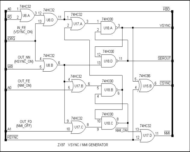
The NMI generator is controlled with OUT FE 🔗 External reference
Related Circuits

Connect the components, ensuring to pay attention to the connections for the transistor. The 22-ohm load resistor and thermistor should be connected in a manner that allows for good thermal contact. Note: If using the Light Application Adapter, REFIN-...
This electronic schematic allows for the design of a simple cellular phone detector circuit capable of sensing the presence of an activated mobile phone from a distance of 1.5 meters. The capacitor C3 should have lead lengths of 18...
As illustrated in the dividing circuit diagram, A1 consists of a voltage-controlled current source, A2 functions as a voltage comparator, and A3 is configured as an active low-pass filter. When the time constant R1C1 is equal to the clock...
The circuit depicted in the figure is a controllable integrating circuit. It features a reset-to-zero function and allows for the adjustment of different integration time constants via a controllable integrator. The analog switch used is C. More specifically, it...
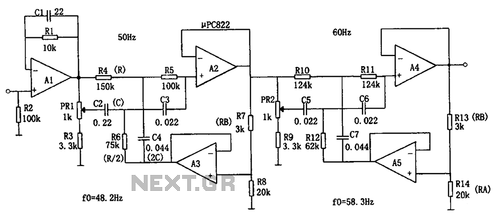
The circuit depicted in the figure is a frequency power supply noise filter circuit, specifically a double-T filter. It is designed to amplify weak signals, such as those from sensors, while filtering out mixed 50Hz (or 60Hz) power supply...
The Dynaco Mark III is the highest power amplifier that was widely sold under the Dynaco name. There was a higher power amp (the Mark VI), but it wasn't widely available. The Dyna MKIII has a basic design flaw...