
Timed Safety Circuit Circuit

The described circuit involves a timing mechanism utilizing operational amplifiers and transistors to control two separate time intervals based on the state of switches. When switch SI is engaged, it triggers a low signal at pin 9 of the operational amplifier U1, which in turn drives transistor Q1 into conduction. This action initiates the first timing cycle, which is determined by the values of resistors R1 and R13. These resistors are configured in such a way that they define the charge and discharge times of a connected timing capacitor, thus establishing the duration for which Q1 remains in the 'on' state.
Simultaneously, if switch S2 is activated while Q1 is conducting, it triggers transistor Q2, which also operates for a specific time period. The timing for Q2 is similarly controlled by the resistor configuration, allowing for precise adjustments to the timing intervals. This dual-timing functionality could be employed in various applications, such as in delay circuits, pulse generators, or timer-based control systems.
The operational amplifier U1 may be configured in a comparator mode, where the input signal from the switch SI is compared against a reference voltage. The output state at pin 9 will transition based on this comparison, ensuring that the timing sequence is initiated correctly. The transistors Q1 and Q2 serve as electronic switches, providing the necessary control to drive loads or other components in the circuit.
In summary, this circuit leverages the properties of operational amplifiers and transistors, along with resistive timing elements, to create a versatile timing solution that can be adjusted for various applications. The careful selection of resistor values R1 and R13 enables precise control over the timing intervals, enhancing the functionality of the overall design. When SI is closed, pin 9 of Ul goes low, turning on Ql for a preset period. If S2 is closed during this period, Q2 is turned on for a preset period. Rl 1 and R13 set the two time periods.
Related Circuits
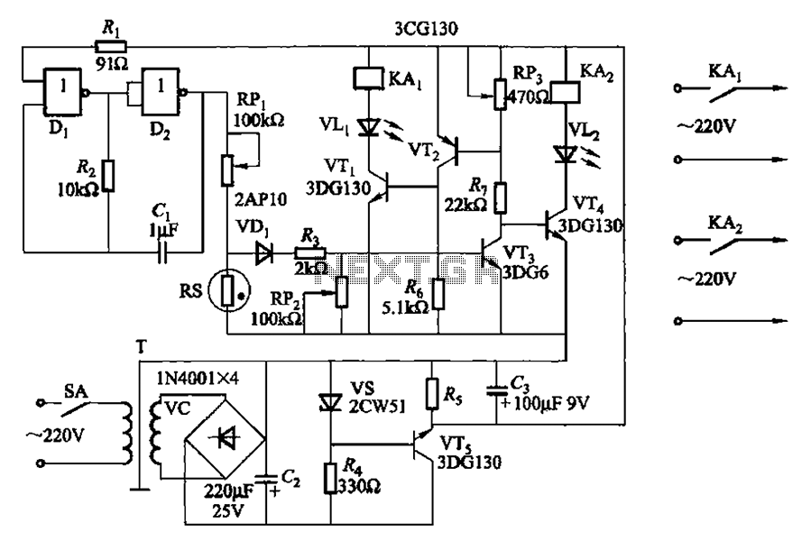
Two NAND gates (Di, Dz) and a resistor (Rz) along with capacitors (C1, etc.) form an RC self-excited multivibrator with an oscillation frequency of 2.5 Hz and an oscillation amplitude of 4 V. This circuit is used as a...
The double-limit temperature alarm circuit consists of a temperature detection control circuit, a temperature indicating circuit, and an alarm sound circuit. The components selected include resistors R1 to R5, which should be 1/4W metal film or carbon film resistors....
The circuit diagram focuses on the research and design features applied to mobile robots. The design considers small size, low power consumption, and ease of movement, catering to home users with a user-friendly display interface. For speech recognition, a...
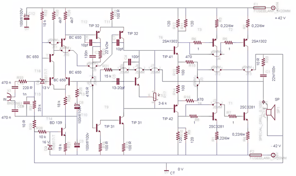
This post presents the circuit schematic diagram for a 500-watt mono power amplifier. As of July 18, 2012, the intention is to create a power sound system with a total output of 1000 watts in stereo. The design utilizes...
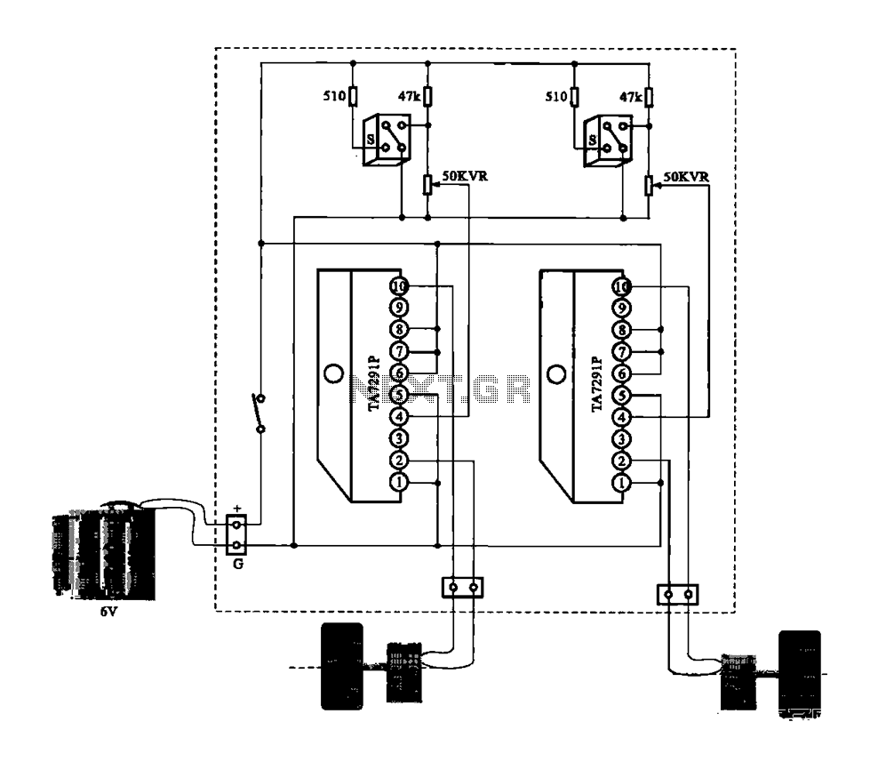
A dual motor drive circuit for automatic tracking consists of two motors that are part of a car structure, which operates based on the principles of a double motor drive system. The dual motor drive circuit is designed to facilitate...
Circuit characteristics: A simple phase shift range of 180 degrees; exhibits good linearity and control accuracy compared to the first two options, making it suitable for low voltage applications, particularly in less demanding electroplating and electrolysis power supplies. The described...