
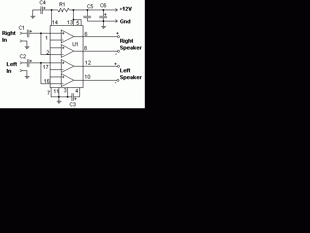
Tone-control audio amplifier
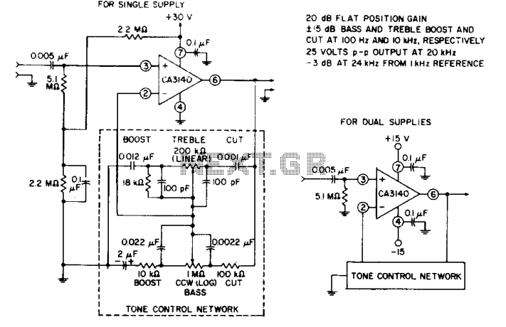
The circuit design leverages the capabilities of the CA3140 BiMOS operational amplifier, which is known for its superior performance in terms of speed and bandwidth. The high slew rate allows for rapid changes in output voltage, making it suitable for applications requiring fast signal processing. The wide bandwidth ensures that the amplifier can handle a broad range of frequencies without significant attenuation, which is critical in high-fidelity audio applications or RF signal processing.
The high input impedance characteristic of the CA3140 minimizes loading effects on the preceding stage, allowing for accurate signal representation without distortion. This feature is particularly beneficial in sensor applications where the source impedance may be high. The output voltage capability of the amplifier ensures that it can drive loads effectively, providing versatility in various circuit configurations.
With a designed gain of eleven, the circuit provides a significant amplification factor, which is essential for applications requiring a strong output signal. The gain is calculated as the ultimate boost or cut plus one, where a 20-dB boost corresponds to a voltage gain of approximately 10, leading to a total gain of eleven when considering the input signal.
In terms of input loading, the resistance from terminal 3 to ground plays a crucial role. For a 20-dB boost or cut, the input loading is effectively determined by this resistance, ensuring that the circuit maintains stability and performance under varying load conditions. This aspect is vital for preserving the integrity of the input signal and ensuring that the amplifier operates within its optimal range.
Overall, this circuit exemplifies the effective application of the CA3140 BiMOS op amp's features, providing a robust solution for signal amplification with minimal distortion and high fidelity.The circuit makes excellent use of the high slew rate, wide bandwidth, high input impedance, and high-output voltage capability of the CA3140 BiMOS op amp. The wideband gain of this circuit is equal to the ultimate boost or cut plus one, in this case a gain of eleven.
For 20-dB boost or cut, input loading is essentially equal to the resistance from terminal 3 to ground. 🔗 External reference
Related Circuits
The TDA2549 is a complete intermediate frequency (IF) circuit that includes automatic frequency control (AFC), automatic gain control (AGC), demodulation, and video preamplification capabilities for multistandard television receivers. It can process both positively and negatively modulated video signals in...
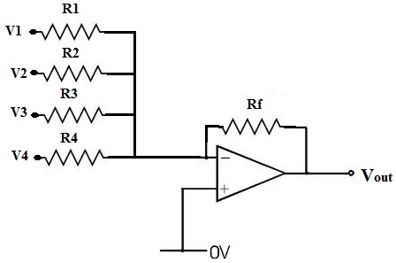
If resistors R1 to R4 are variable, the signals can be mixed in any proportion, allowing for adjustments at various volume levels. The overall volume can be controlled using a variable resistor in series with Rf. In this circuit configuration,...
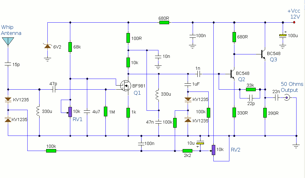
The antenna amplifier circuit comprises approximately 40 components, featuring two NPN transistors (BC548), one MOSFET (BF981), two varicap diodes (KV1235), and a 6.2V zener diode. It includes a 330µH inductor/coil, which can be modified for operation on different frequency...
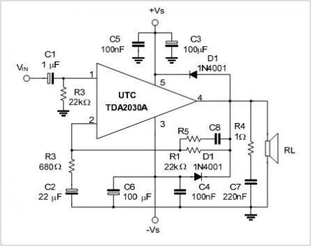
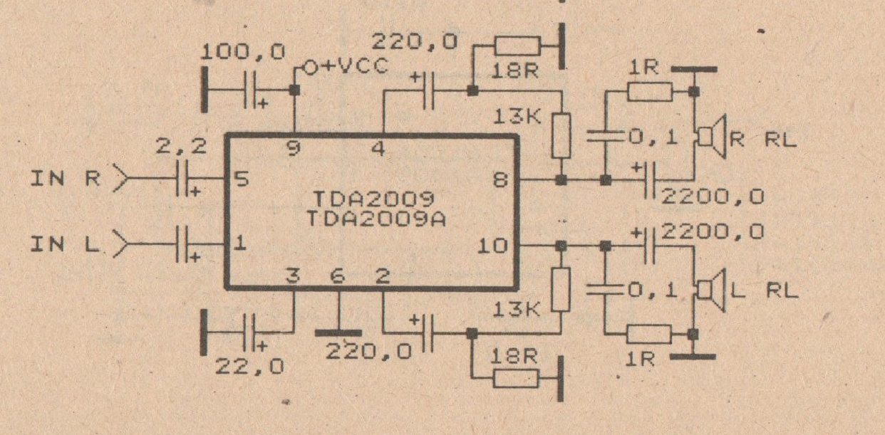
This is a stereo power amplifier circuit that operates at up to 22W per channel, resulting in a total output of 2x22W. A few external components are required to support the main component, the TDA1554. A heatsink on the...
The minimum voltage required for this circuit is 8 volts, while the maximum voltage is 28 volts. It can be used to amplify audio signals in electronic devices such as radios, DVDs, MP4 players, and MP5 players. The circuit...
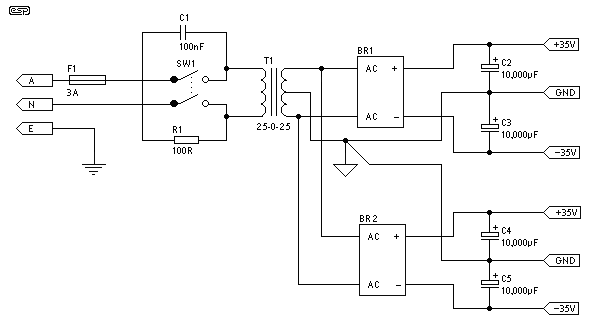
To order boards, click to access the ESP Purchase form. Verify the price and postage, then open the order form, fill it in, and print it from your browser. Boards are sold only as a stereo pair and are...