
Totem-Pole Output configuration found in ICs
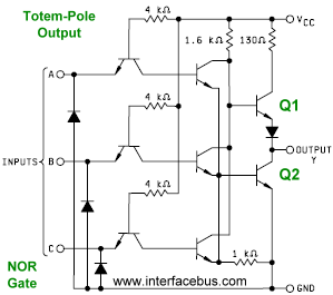
Totem-Pole Outputs are a fundamental design choice in digital logic circuits, particularly in TTL (Transistor-Transistor Logic) families. The architecture consists of two bipolar junction transistors (BJTs), where Q1 is responsible for pulling the output high and Q2 for pulling it low. This arrangement allows for a strong drive capability in both the high and low states, which is crucial for interfacing with other digital components.
In a typical application, when the input conditions dictate a high output, Q1 is activated, allowing current to flow from the positive supply voltage (Vcc) to the output. This creates a low impedance path to the load, ensuring that the output can drive multiple connected devices without significant voltage drop. Conversely, when the output is required to be low, Q2 is turned on, providing a direct path to ground and sinking current from the output. This dual action minimizes the time it takes for the output to transition between states, enhancing the overall speed of the circuit.
The rise and fall times of the output pulse are critical parameters in digital circuit design. The presence of additional components, such as resistors or capacitors, in conjunction with Q1 and Q2 can affect these timings. For instance, if a resistor is placed in series with Q1, it will slow down the rise time because it adds additional resistance to the current flow. Similarly, any capacitance at the output will introduce a time constant that affects how quickly the output can change state.
Different logic families, such as CMOS or ECL, may implement variations of the Totem-Pole configuration, leading to differences in output drive strength, power consumption, and speed. Understanding these variations is essential for selecting the appropriate logic family for specific applications, especially in high-speed digital circuits where performance metrics are critical.
In summary, the Totem-Pole Output configuration is a widely used output structure in integrated circuits, characterized by its ability to efficiently drive high and low outputs through a pair of transistors, Q1 and Q2. Its design considerations, including rise and fall times, are vital for ensuring reliable operation in digital applications.A type of output structure used with integrated circuits in which one transistor drives the output high while another transistor connected below it pulls the output low. Many ICs use Totem-Pole Outputs, in fact it`s so common that the output structure isn`t mentioned in the data sheet title.
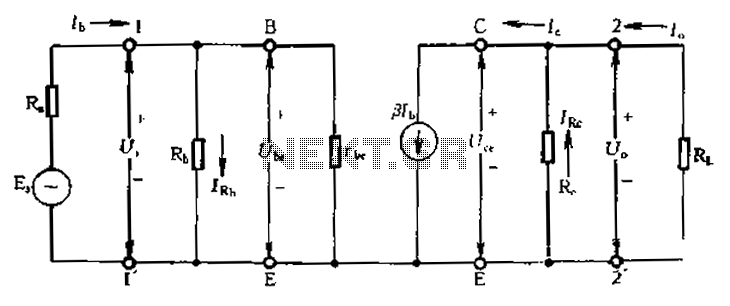
An IC with a Totem-Pole Output is the default condition. As opposed to an Open Collector Output which is always indicated in the title of the data sheet. The circuit schematic shown below details the internal structure of a TTL triple input NOR gate with a Totem-Pole Output. The Totem-Pole is formed by transistors Q1 and Q2. The schematic and logic diagram are examples of 3-input NOR gates. The output structure will be some deviation of a Totem-Pole but the actual schematic will change depending upon the Logic Family used.
Note that the current paths are different between a high and low pulse. A totem-pole output sources current out to the load and sinks current in. Or an output high is derived from Vcc through Q1, and an output low is derived from Q2 to ground. So a rising pulse sees the impedance path of Q1 while a falling pulse see the impedance path of Q2. Depending on the logic function and the logic family there may be components in one or both paths in addition to the switching transistors Q1 and Q2. The different components and the different impedances of the transistors causes a difference between the rise time and the fall time of the output pulse.
🔗 External reference
Related Circuits
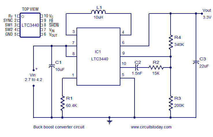
A simple and highly efficient buck-boost converter is implemented using the LTC3440 integrated circuit. The output voltage is set at 3.3V, while the input voltage range can vary from 2.7V to 4.2V. The LTC3440 is a synchronous buck-boost converter designed...
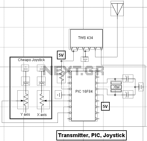
With a handful of inexpensive components, a little creativity, and the power of PicBasic, you can build some pretty outstanding robotics creations as Rob Arnold proves with his Ruf-Bot project. RF remote control is just way too cool not...
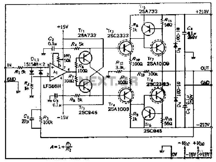
This amplifier circuit operates with an OP amplifier that is power-driven, which leads to the presence of floating voltage errors and necessitates a high-pressure booster for transistor protection. The circuit utilizes a mutual feedback configuration, connecting to the output...
Calculate magnification, input resistance, and output resistance circuit. This circuit is designed to calculate the magnification, input resistance, and output resistance of a given electronic system. The magnification refers to the ratio of the output signal to the input signal,...
This tutorial continues the discussion on 8051 Assembly Programming by teaching input and output instructions for 8051 microcontrollers using assembly language. The microcontroller comprises a total of forty pins, most of which serve multiple functions. The primary function is...
BEAM enthusiasts often quickly learn to scavenge necessary components for their projects from technoscrap. However, there will always be occasions when purchasing new parts or materials becomes essential. This trend is increasingly prevalent as Application Specific Chips are being...
Warning: include(partials/cookie-banner.php): Failed to open stream: Permission denied in /var/www/html/nextgr/view-circuit.php on line 713
Warning: include(): Failed opening 'partials/cookie-banner.php' for inclusion (include_path='.:/usr/share/php') in /var/www/html/nextgr/view-circuit.php on line 713