
Available voltage booster 400Vp-p output

This amplifier circuit is designed to operate efficiently while addressing potential issues associated with floating voltage errors. The use of an operational amplifier (OP) ensures that the circuit can maintain its functionality under varying conditions. The high-pressure booster serves to stabilize the voltage levels, protecting the transistors from damage due to fluctuations.
The mutual feedback configuration enhances signal integrity by allowing for better control over the output circuit. The absence of home bias and the inclusion of a water compensation circuit contribute to the overall stability of the amplifier. The push-pull configuration of the high-voltage transistors ensures that both halves of the waveform are amplified effectively, leading to improved output performance.
The two-stage DC-coupled circuit is a critical aspect of the design, as it allows for significant voltage gain while minimizing distortion. The negative feedback applied in the output stage helps to maintain linearity and stability, which is essential for high-fidelity audio applications.
The inclusion of a small resistance in the power amplifier circuit serves as a precautionary measure against short-circuit conditions. In cases where a negative short-circuit current occurs, the protective circuit activates to limit the current, preventing damage to the output transistors. This current limit is carefully calibrated to approximately 10 mA, ensuring that the circuit remains within safe operating conditions.
Diodes are strategically placed within the circuit to absorb any ripple voltage generated during operation. These diodes perform a clamping function, ensuring that any excess voltage does not interfere with the circuit's performance. Overall, this amplifier circuit is designed with a focus on reliability, safety, and high performance, making it suitable for a variety of applications. Because this amplifier circuit OP mountain with isv power-driven, so sad existence as floating voltage error plus high pressure booster as a disc insurance o transistor Tri, TT J is mutual bashing shot summarized follower, this will be connected to the output circuit It would be more reasonable (no home bias, still water compensation circuit). High voltage transistor Tt, Tr to complete the transfer of a high voltage, in order to raise high soil line, and Used the push-pull mode.
To learn Cantonese peak locust static pressure as much as possible close to the supply voltage, the output transistor T ,. Ding, Trrb then lied shot Terrier ground circuit., By the Tr. Tr, (Tr4. Tr8) DC-coupled two-stage circuit, because the voltage gain is large, so the output stage negative feedback.
Closed-loop magnification static milli Guangdong times ( r F iso lI/z four soil), is to encourage the greater use OP. Ran lose 1 small resistance of power amplifier circuit, when there is a negative short-circuit current cut Luk frog, the output transistor is damaged, and therefore, we need to take to protect streams, Tr5, 1 prison..
Hang from the Qing limit the role of the protective circuit. Luk limit current IL Wang dish can be thrown -l V. 1. Workers, r amount./Island formula is obtained. Possession of the current limit circuit is about lOmA. Connected to the output terminal and Chrysler to good electrical ov lim of the diode D ugly, D play a clamping action to absorb the ripple voltage profile tallow produced.
Related Circuits
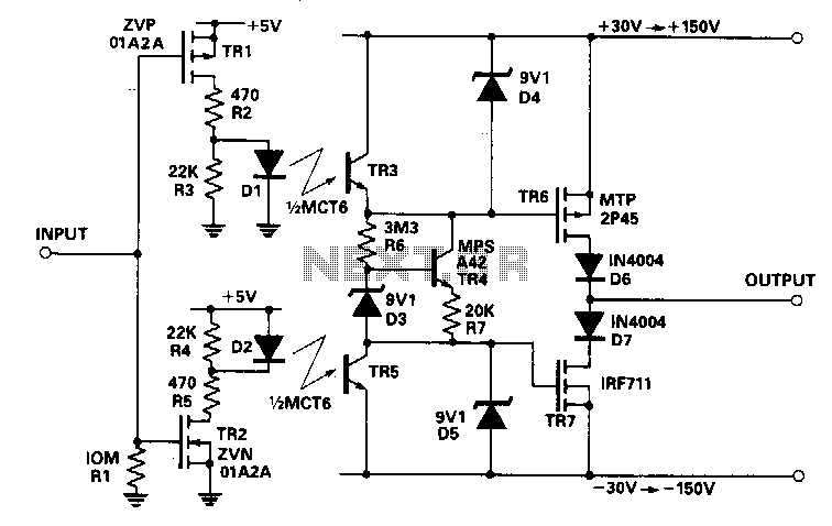
This circuit accepts a signal from a 5-V CMOS logic circuit and produces a high voltage of the same polarity. The high-voltage supply can be adjusted between ±30 V and ±150 V without requiring any changes to the circuit...
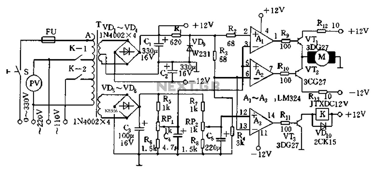
Automatic AC voltage regulator circuit TXD1742 with continuous adjustment. The TXD1742 is an automatic AC voltage regulator circuit designed to provide continuous voltage adjustment, ensuring stable output voltage in varying load conditions. This circuit is particularly useful in applications where...
Opamps are very useful. But one of their major drawbacks is the requirement of a dual supply. This seriously limits their applications in fields where a dual supply is not affordable or not practicable. This circuit solves the problem...
The goal is to take the voltage output from a 3.5mm audio jack and use it to light up an LED based on the audio voltage levels. The left audio channel will be connected to the base of a...
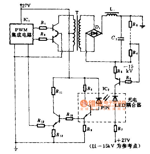
The technical parameters of high-speed optocouplers include a rise time (t1) of less than or equal to 300 ns, a circuit transfer ratio (CTR) of 50%, an isolation voltage (VSO) of at least 15,000 V, and an output transistor...
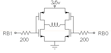
Drive a small (3.6V, <1A) brushed motor bidirectionally with a PIC microcontroller (MCU). The available space is extremely limited, so a single 3.6V power supply will be used for both the motor and the PIC, with minimal drive circuitry required. There is no dedicated motor driver IC that operates at this low voltage, making a discrete H-bridge the most suitable drive arrangement. The NXP PMV30UN and PMV32UP have been identified as suitable N-type and P-type drive MOSFETs. Since both the PIC and the motor share the same power supply, it is questioned whether it is possible to eliminate the usual driving circuitry for an H-bridge and connect the transistors directly to the MCU pins. Potential pitfalls of this approach should also be considered. To design a bidirectional motor drive circuit using a PIC microcontroller and a discrete H-bridge configuration, the following considerations must be taken into account. The H-bridge consists of four MOSFETs arranged in a configuration that allows current to flow through the motor in either direction, enabling bidirectional control. The NXP PMV30UN and PMV32UP MOSFETs are suitable candidates due to their low on-resistance and capability to operate at the required 3.6V supply voltage. The connections between the PIC MCU and the MOSFETs should be made with consideration of the gate drive requirements. Directly connecting the MOSFET gates to the MCU pins can be feasible, but it is essential to ensure that the MCU can provide sufficient gate drive voltage to fully turn on the MOSFETs. A typical threshold voltage for these MOSFETs is around 1V, so the output high level from the PIC should exceed this threshold to ensure efficient operation. It is also critical to incorporate pull-down resistors on the gate pins to prevent the MOSFETs from floating when the MCU is in a high-impedance state. This will help avoid unintended motor activation. Additionally, using gate resistors can help dampen any oscillations and limit inrush current during switching, which could potentially damage the MOSFETs or the MCU. Another consideration is the back EMF generated by the motor when it is switched off or when changing direction. This can induce voltage spikes that may damage the MCU or the MOSFETs. To mitigate this risk, flyback diodes should be placed in parallel with each MOSFET to provide a path for the back EMF, ensuring safe operation of the circuit. Thermal management is also a critical aspect of the design. Although the MOSFETs are rated for low on-resistance, continuous operation near their current limits can lead to significant heat generation. Adequate heat dissipation measures, such as heat sinks or thermal pads, should be considered. In summary, while it is possible to connect the MOSFETs directly to the MCU pins, careful attention must be given to gate drive requirements, protection against back EMF, and thermal management to ensure reliable and efficient operation of the bidirectional motor drive circuit.