
Touch Screen Model

The capacitive touch screen model described involves a sophisticated interplay of physical and electrical parameters. The primary components include the transparent conductors, which are typically made from materials such as indium tin oxide (ITO) due to their excellent conductivity and transparency. The arrangement of these conductors is critical, as their perpendicular orientation maximizes the area of overlap, thereby enhancing the sensitivity of the touch screen.
The modeling of a user's finger is crucial, as it introduces a variable capacitance that significantly affects the overall performance of the touch screen. The finger's proximity alters the electric field between the conductors, effectively changing the capacitance and leading to the phase shift detected by the circuitry. The demodulation process is essential for translating the phase shift into a usable signal. A typical demodulator circuit may utilize operational amplifiers to process the incoming signals, ensuring that the variations in capacitance due to touch are accurately converted into a digital signal that can be interpreted by a microcontroller.
To optimize the design, advanced simulation tools can be employed to model the capacitive interactions dynamically. These tools can facilitate real-time adjustments to parameters such as conductor spacing, material properties, and signal frequencies, enabling a more responsive design process. By implementing a feedback loop within the simulation, designers can iteratively refine the touch screen model based on performance metrics derived from initial tests, thereby enhancing the accuracy and reliability of touch detection.
In conclusion, the development of a capacitive touch screen model involves a comprehensive understanding of both the electrical and physical aspects of the system. By leveraging advanced modeling techniques and circuit design principles, it is possible to create a highly responsive and accurate touch interface suitable for a wide range of applications.The challenge of this project is to create a model of a capacitive touch screen, including physical modeling of a user`s finger, the touch screen materials, and the touch-detection circuitry. A capacitive touch screen works by measuring the change in capacitance between two conductors caused by a nearby finger.
In the touch screen, two transparent conductors, which run in perpendicular directions, are separated by the screen. These conductors act as a parallel-plate capacitor where they overlap; the capacitance is determined by numerous physical parameters. For example, the conductor width, length, resistivity, and separation, along with the screen material properties and thickness, all affect the coupling between the conductors.
To operate a single pixel of the touch screen, a particular frequency is transmitted along one conductor and received by the other. The capacitive coupling between the conductors causes a particular phase shift in the received signal.
When a finger is close enough to where the conductors overlap, it changes the capacitance between the conductors because the finger appears to be grounded. This causes an additional phase shift, which is detected by a simple demodulator circuit and converted into a DC signal.
When the DC signal exceeds a given threshold, a touch is detected by the pixel. This process occurs for all of the touch screen pixels to determine which locations are being touched. The traditional approach to modeling a touch screen uses a purely circuit-based design that uses components whose values must be precomputed in another environment.
Changes in the design parameters would require the recalculation and re-entry of these and other values into the circuit model before subsequent simulations; this process makes experimentation and fine-tuning of the model difficult and time-consuming. For example, the coupling capacitance between the transmitting and receiving conductors would have to be calculated and fed into the circuit simulation ahead of time.
Similarly, the effect of a grounded finger would have to be incorporated as some time-dependent capacitance whose time-domain waveform is predetermined and loaded into the simulator. Also, the demodulator, which is essentially the multiplication of two sine waves, would have to be implemented using a full demodulator circuit as opposed to simply multiplying two signals.
🔗 External reference
Related Circuits
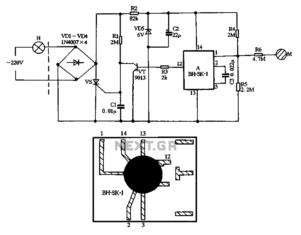
The BH-SK-I is a touch light switch circuit that integrates a single bond voice integrated circuit. The circuit is divided into two sections: the left section represents the general lighting lines, while the right section illustrates the touch switch....
The objective is to demonstrate that the electrical field energy produced by a well-designed Tesla coil transmitter can be detected by a sensitive, well-tuned Tesla coil receiver placed at distances exceeding a few wavelengths. The current investigations involve scaled-down...

Mindsensors produces an excellent RCX sensor multiplexer for the NXT, known as the RXMux, which enables the connection of up to four RCX-style analog sensors to the NXT. The RXMux supports various sensors. Due to the frequent use of...
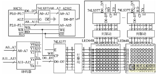
This document outlines the theory behind a high-speed control scheme for an LED display screen circuit. The circuit utilizes the MCS51 series microcontroller to manage the LED display. A 62512 random access memory (RAM) is employed for data storage,...
Typical solutions for the vertical movement of probes in bed profiling devices include guide wheels, dumpers, brakes, and vibration suppressors (not shown). A complete mechanism for vertical motion of a bed profiler is illustrated, featuring an electric motor, a...
The objective is to establish a space dedicated to art, audio, and video, centered around a vintage electronics theme. The vacuum tube is considered the core component of any vintage radio or electronic device. Currently, the usage of vacuum...