
High-speed control scheme LED display screen circuit diagram and principle
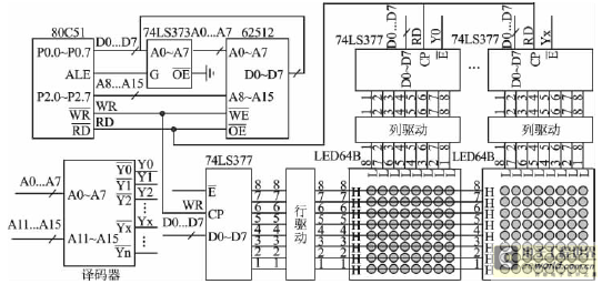
The LED display circuit operates on a high-speed control scheme that integrates a microcontroller from the MCS51 series, which is responsible for managing the display's functionality. The choice of a 62512 RAM for data storage allows for efficient handling of the matrix data that represents the visual output. The architecture employs an 8-line scanning mode, which is essential for controlling the LED segments effectively.
Each LED dot matrix slice is equipped with a dedicated driving circuit, which is critical for ensuring that the display operates smoothly and accurately. The use of the 74LS377 latch enables the CPU to store and transfer matrix data to the driving circuits through a parallel bus, facilitating rapid data exchange. The address decoder circuit plays a pivotal role in managing the selection signals for both the LED dot matrix and the driving circuits, ensuring that the correct data is sent to the appropriate segments of the display.
One of the innovative aspects of this design is the control of the latching signal via the RD control signal instead of the conventional WR signal. This modification allows for a more streamlined operation, as the CPU can execute read operations more efficiently. Furthermore, the address decoder ensures that the chip selection addresses do not overlap with the logical addresses of the data storage, preventing any potential conflicts and enhancing the reliability of the system.
The operational flow begins with the loading of the data address into the DPTR register, followed by the execution of the MOVXA, @DPTR instruction. This instruction is crucial as it enables the CPU to read the matrix data stored externally and load it into the accumulator A. The unique addressing scheme allows the DPTR to simultaneously reference an external data storage address and a specific latch for the LED dot matrix. When the latch receives a pulse during this operation, it effectively locks in the matrix data, ensuring that the display output is accurate and timely.
The RD control signal, which is utilized during the execution of the MOVXA instruction, replaces the traditional WR signal for latching purposes. This dual functionality enhances the speed of the display control process, allowing for a significant reduction in the time required to write matrix data to the LED display. The previous requirement of over ten seconds for data writing has been drastically reduced to just four seconds, showcasing the efficiency improvements achieved through this design.
In summary, the high-speed control scheme for the LED display screen circuit represents a significant advancement in display technology, utilizing a combination of effective memory management, innovative control signals, and efficient data handling to achieve rapid and accurate visual output.This is a high-speed control scheme LED display screen circuit theory. Adopt the MCS51 series one-chip computer to control LED display screen; The random access memory 62512 is used as the data storage of LED display screen, store the matrix data waiting to reveal the content; Adopt 8 lines of scanning modes, the dot matrix of lamellar LED is a scene of sharing and a group driving circuit; Each slice of LED dot matrix slice has a series of lines of driving circuit, use 74LS377 As listing the latch that is driven, CPU writes the matrix data to the latch which lists the driving circuit through the parallel bus; The decoder circuit of the address, used for producing LED dot matrix slice walking driving circuit and chip selection address which lists the driving circuit. There are two characteristics of this scheme: First, though CPU still gives and lists the latch of the driving circuit and writes the matrix data through the parallel bus, but the latching the control signal RD that the signal uses CPU instead, but not WR of the regular usage of the latch; Second, address decoder circuit guaranteed LED dot matrix a chip selection address which lists the driving circuit and logic address of some segment of the data storage are eclipsed, but not regular usage, these two group addresses must be separated.
Because above-mentioned some of circuit change briefly, one-chip computer take place obvious change to the intersection of LED and the intersection of presentation control and efficiency of display screen. The concrete working phase is as follows: Having already packed into the address of the data storage while assuming the indicator DPTR of the data, execute instruction MOVXA, @DPTR .
The function of this order is CPU, according to pointing to reading the matrix data from the external data storage of DPTR, read it in the accumulator A; But in this circuit, because LED dot matrix a chip selection address which lists the driving circuit and logic address of some segment of the data storage are eclipsed, that is to say, in execute instruction MOVXA, @ DPTR When, DPTR, besides pointing to a certain address of the external data storage, chooses dot matrix slice of a certain LED to list the latch of the driving circuit. If the latching the pin and just throwing into pulses of this latch chosen at this moment, then the latch just locks the matrix data sent from the external data storage.
The one that threw into the pulse and used is RD. RD is CPU in execute instruction MOVXA, @ DPTR The ones that sent out to the external data storage hour read the control signal. Because the reading the control signal RD and writing the sequence of the control signal WR is all the same [2 ] of MCS51 series one-chip computer, RD realizes and latches the function instead of WR, certainly just have no suspense.
This order is during execution, while finishing studying in the data storage, the ones that have finished to LED dot matrix slice are written, so has accelerated the course of presentation control. In the front say CPU finish 1 write the machine format procedure course of the matrix to the intersection of LED and the intersection of dot matrix and the intersection of row and latch of driving circuit of slice at the parallel bus, probably need more than ten s; Now 4 s only, quickly getting many, finish 1 write matrix machine format procedure course need only two steps to the intersection of LED and the intersection of dot matrix and the intersection of row and latch of driving circuit of slice now, compose the actual address, continue CPU according to the pointing to and reading the matrix data from the external data storage of DPTR for the indicator DPTR of the data at first, it is said, give LED the intersection of dot matrix and slice to list latch of driving circuit the intersection of word and modulus at the same time with it.
2 orders, 4 machine cycles, 4 s. Want some of 🔗 External reference
Related Circuits
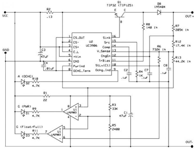
The UC3906 battery charger circuit controller includes all necessary circuitry to manage the charge and hold cycles for sealed lead-acid batteries. This circuit is specifically designed to deliver the appropriate charging voltage and current based on the battery's temperature...
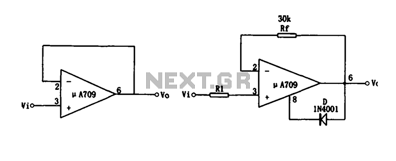
Figure (a) illustrates a voltage follower circuit, which serves as a specific instance of an in-phase amplifying circuit. The input signal originates from an integrated operational amplifier. At the conclusion of the introduction phase, the feedback resistor is set...
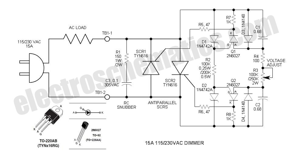
The DIAC is a 28V bidirectional trigger device commonly used in inexpensive phase control applications. Its trigger voltage is relatively high for 115VAC phase control. In the past, a similar low voltage trigger device known as a Shockley diode...
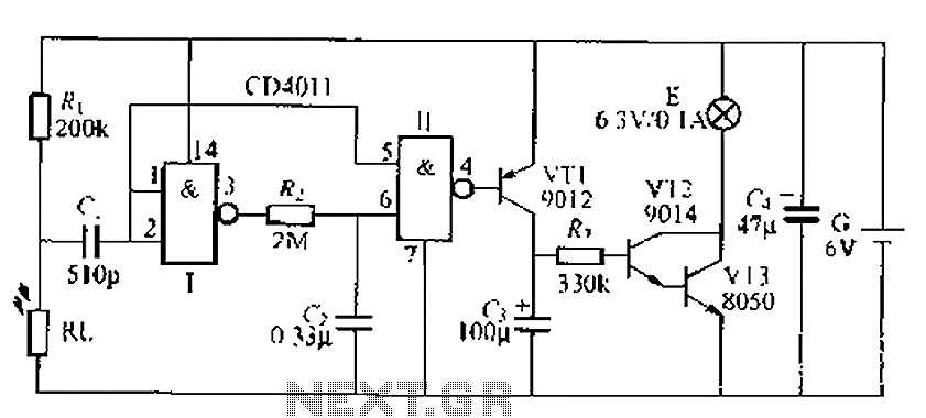
A battery-powered light control circuit is designed to delay the lighting of a small lamp during sudden power outages or nighttime situations when a blown fuse leaves a room in darkness. This circuit addresses the difficulty of locating matches...
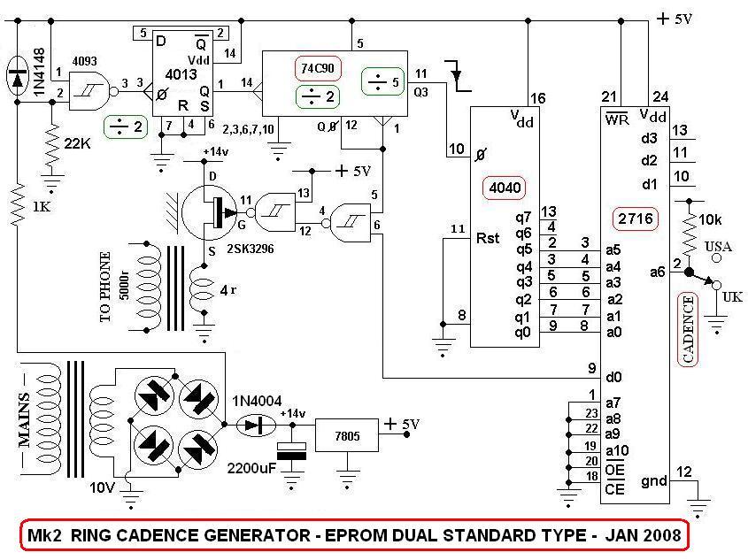
This is a switch-selectable dual output version of a previous design from 2007, utilizing a field-programmed EPROM to generate two versions of the ringing sequence. The AC mains voltage is stepped down to approximately 10 V AC and then...
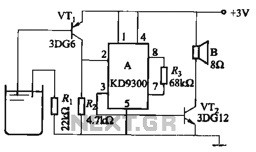
Changing the values of Ri, R2, Cl, and C3 can modify the alarm tone. The circuit utilizes KD9300 music integrated circuits. The circuit described is designed to generate an alarm tone through the manipulation of specific component values within the...