
Transistor Radio Output Stages

These are the standard line-ups, and most early MW/LW sets will have either six or seven transistors depending on the model and original selling price. Because the class AB output stage current consumption varies with the signal being amplified, the current drawn from the supply (battery) varies in sympathy.
This will cause the supply voltage to fluctuate. We need to prevent these rapid fluctuations from finding their way back to the driver and earlier stages, otherwise they could cause distortion and/or instability. In the circuit above we have a 100uF capacitor (C7) directly across the power supply. This would be mounted close to the output stage and would smooth the fluctuations. The supply to the driver stage biasing and earlier stages in the set is further filtered or decoupled by a 1k-ohm resistor (R13) and another 100uF capacitor (C5).
If this capacitor fails the set will probably make a horrible noise known as "motor-boating" because it resembles the sound of an outboard motor. If the 100uF capacitor directly across the power supply were to fail the same effect would probably occur but only as the battery starts to run down.
The main problem with the two-transformer circuit above is the cost and weight of the output transformer. This is a particular problem with higher quality sets, because good quality output transformers tended to be larger and more expensive than lower quality types.
If a set is built on a PCB you really don`t want a big heavy lump of metal mounted on it. The driver transformer only has to deal with signals, not power, so it will be smaller and less of a quality or weight problem. This circuit shows the basic arrangement of a single transformer class AB output stage. It may also be called a direct-coupled output stage since the speaker is directly connected to the transistors.
The two transistors are connected in series across the supply and individually biased. The transistor bases are driven by individual windings on the driver transformer. The central point in the circuit (between the two transistors) will be at half the supply voltage with no signal, and will vary above and below with the signal. If two batteries are used in series, as shown in solid line, the central point between them will also be at half supply voltage, so the other side of the speaker (RL) may be connected to here.
More often however a single battery will be used, so the speaker will be returned to one side of the supply and an electrolytic capacitor will be used for DC blocking and AC signal coupling (shown dotted). If this capacitor fails the output will become weak and/or distorted. The main problem with this circuit is the need for a higher impedance speaker - typically between 25 and 75 ohms.
These are more difficult and expensive to produce than standard 4 or 8 ohm units, which negates some of the cost saving from eliminating the output transformer. This circuit shows a practical implementation of this arrangement. This is a Mullard reference circuit and is typical of the circuit and component values that will be encountered in many sets.
The bias resistors marked * are specified at 5% tolerance, other resistors are 10%. Negative feedback is applied around the whole circuit from the output to the emitter of the driver transistor by the 2. 7k resistor at the bottom. The various 🔗 External reference
Related Circuits
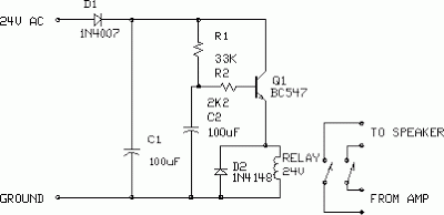
This is a minimal circuit designed for individual audio amplifier projects to control the presenter output relay. The purpose of this circuit is to manage the relay that activates the speaker output within the audio amplifier. The circuit introduces...
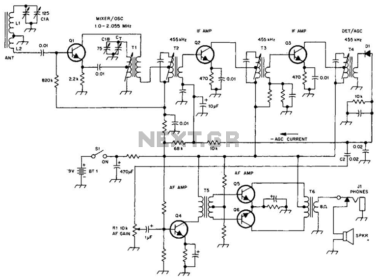
A schematic of a typical transistor AM radio is presented. This circuit utilizes npn transistors. It is a generic circuit; hence, specific values for some components are not provided. This circuit serves as a reference point for experimenters. The schematic...
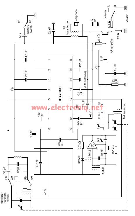
The TDA7088 features a frequency-locked-loop (FLL) system with an Intermediate Frequency (IF) of approximately 70 kHz. This circuit can be powered using a 3-volt battery cell or a regulated power supply. The TDA7088 is a highly integrated FM radio receiver...
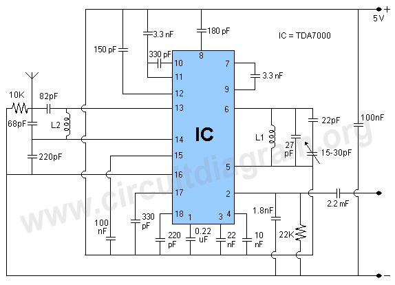
The TDA7000 is a well-known FM radio receiver integrated circuit (IC), also referred to as a one-chip FM radio receiver. It operates within the VHF FM band, covering frequencies from 70 to 120 MHz. Introduced in the 1980s, the...
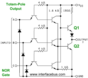
A type of output structure used with integrated circuits in which one transistor drives the output high while another transistor connected below it pulls the output low. Many integrated circuits utilize Totem-Pole Outputs; in fact, it is so common...
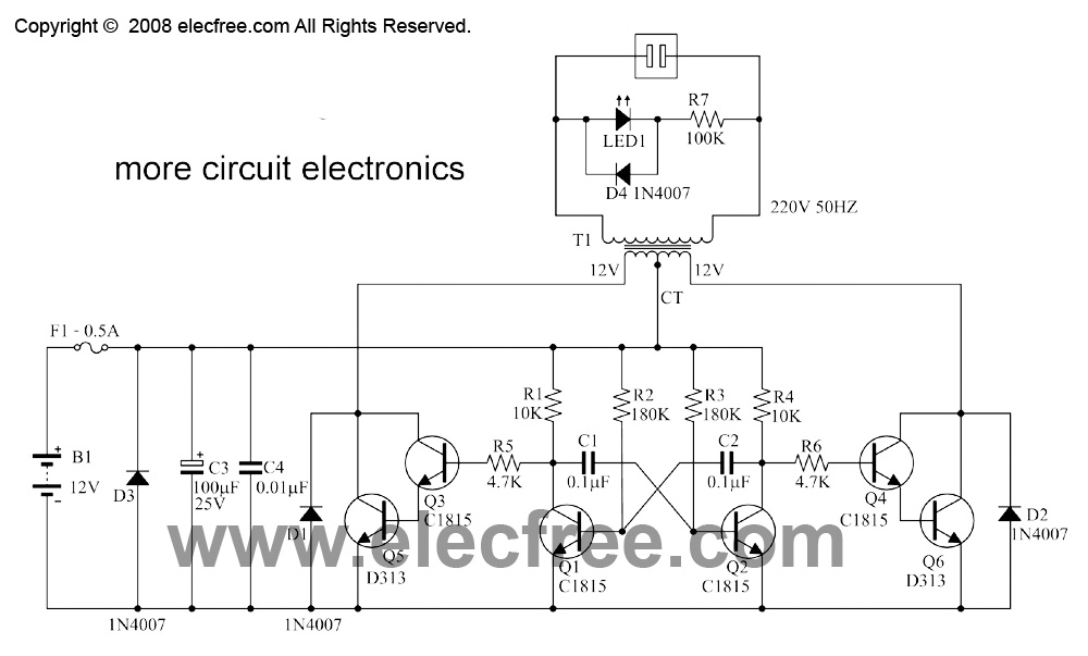
This is a small inverter rated at 30 watts. It converts DC voltage from a 12V battery to AC voltage of 220V-230V at a frequency of 50Hz, which is the same electricity used in households. It can power 2-3...