
Transistor regulator circuit can adjustable output voltage
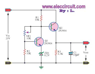
The circuit can be divided into several key components, each serving a specific purpose. The Q1 transistor operates in a common-emitter configuration, which is crucial for voltage amplification and regulation. The base-emitter junction of Q1 regulates the input voltage by maintaining a fixed voltage drop of approximately 0.6 V, allowing for effective control over the output voltage.
The zener diode ZD1 plays a critical role in voltage regulation by providing a stable reference voltage of 6.2 V. This voltage, in conjunction with the base-emitter voltage of Q1, establishes a reliable operating point for the circuit. The adjustable resistor VR1 allows for fine-tuning of the output voltage, enabling the user to set the desired voltage level within the specified range.
The Q2 transistor, also in a common-emitter configuration, acts as a power supply current source, ensuring that the circuit can deliver the required output current while maintaining voltage stability. The biasing of Q2 through the base pin allows for effective control of the output voltage, further enhanced by the use of the adjustable resistor VR1.
The inclusion of R3 and C1 as an RC filter is essential for minimizing voltage ripple, ensuring that the output voltage remains stable and free from fluctuations. This is particularly important in low current applications where precision is required.
Overall, this circuit design is optimized for low current applications, providing a simple yet effective means of maintaining a constant output voltage while minimizing the effects of temperature variations. The careful selection of components and their configurations contributes to the reliability and performance of the circuit.This circuit is maintain a constant voltage, the output voltage is adjustable. Serves to reduce the input voltage, and keep the voltage constant. The Q1 2N3904 is the amplifier model. common-emitter. This causes the voltage across the collector`s pin with the ground. Is equal to the voltage between the legs to the ground base of Q1. The volt base-em itter (0. 6 V), the zener diode volt (6. 2 V), then adjust the voltage VR1. This circuit has a temperature coefficient is very little, almost zero. The joint base emitter of Q1 with a temperature coefficient of -2 mV per Degree Celsius And zener didoe ZD1 have the temperature coefficient of +2 mV per degree Celsius. Reduce the effect of temperature on the circuit. The Q2 to drive the output up. However, the output voltage drops, which can be adjusted with VR1 voltage range 6. 8 15. 6V. The R3 and C1 act as RC filters, voltage ripple less. But this circuit is less than 100 mA current only, is ideal for low current circuits. This again the one circuit that use in fining value output voltage, for apply give straight with the requirement of load be the circuit that is simple and have no result temperature way of the joint junction of transistor.
Vout control 0V-30V at 0. 1A The principle works be transistor Q1 2SC458 that built model common-emitter amplifier, which perform fine decrease input voltage get down then heal volt that give may but at collector voltage compare with ground. Which get from the combination of voltage at base emitter pin (0. 6V) with VZener diode (6. 2V) already fine the value of a resister can fine the value VR1 help transistor part Q2 2SC458 perform be compared as power supply current source and current that fixed.
By current at flow come in the way base pin of Q2 and when Q2 bias current. That already Voltage output get, with fining that a resister VR1 during 5. 8V-15. 8V. By have R3 and C1 perform be RC Filter caution. This circuit power current source get 100mA topmost should apply to load that use current low. 🔗 External reference
Related Circuits
This circuit creates an impressive display of magnetism by suspending a small metal object in mid-air. Utilizing an electromagnet, a photo sensor, and a closed-loop control system, lightweight metal objects can be levitated just beneath the magnet, enclosed in...
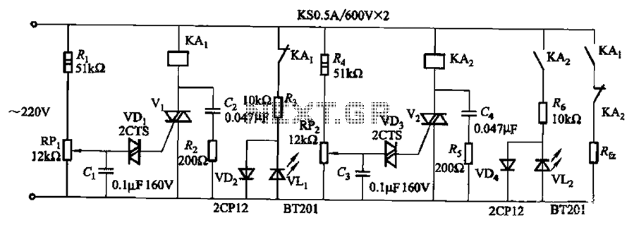
Bidirectional thyristor control. By adjusting potentiometers RPi and RPz, the lower and upper limit values can be changed. LEDs VLi and VL2 serve as indicators for low pressure and high pressure, respectively. The circuit utilizes a bidirectional thyristor to control...
The capability to control lights and fans wirelessly has transitioned from an expensive luxury to widely accessible consumer solutions. Nevertheless, creating a custom solution remains an engaging project for hobbyists and tinkerers. RobotGrrl has developed user-friendly libraries aimed at...
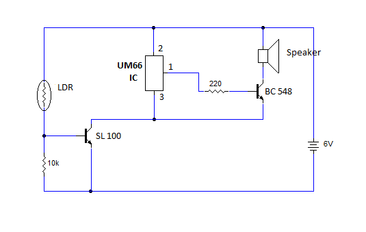
This article provides instructions for creating a light-sensitive morning alarm circuit. The circuit utilizes an LDR (Light Dependent Resistor) or photoresistor to detect morning light, which triggers the alarm section. When light is detected, the circuit produces a melodious...
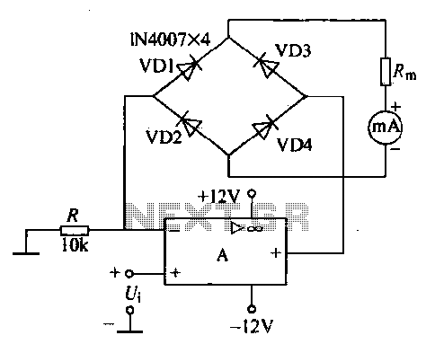
An operational amplifier, a diode bridge rectifier, and DC mA AC voltmeter tables are illustrated in the figure. The operational amplifier used is the LM324. The measured AC voltage is applied to the inverting terminal of the operational amplifier,...
This regulated power supply is adjustable between a few volts and 15V using P1, while P2 is used to set the upper limit at 15.0V. The value of R6 is calculated as 0.7V divided by Imax, where Imax represents...