
Transistor tester circuit
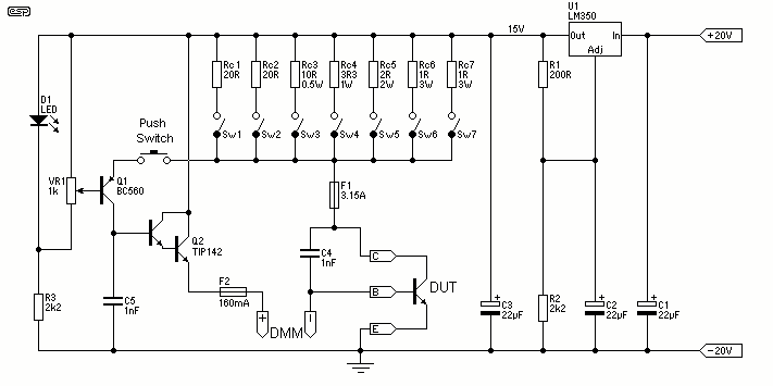
Fuse F1 provides protection from high collector currents and has been fitted where shown, rather than in the supply rail, so that a 3.15A fuse can be used. If fitted in the supply rail, the next higher standard value (4A) would be needed, thus providing reduced protection. This is because the base current would also be passing through the fuse if it were in the supply rail.
Fuse F2 has been provided to prevent excess base current in the event of the DUT being faulty or incorrectly connected. A resistor in the collector of Q2 could achieve a similar effect, but, if large enough to provide sufficient current limiting, the DUT collector current variation for low gain transistors would be outside the design objective of keeping the current constant (for different DUT hFE) to within 1%. A lower value collector resistor for Q2, such that the DUT collector current remained constant, would not limit the DUT base current to below 0.5A and would need to be rated at 10W to prevent failure under fault conditions.
C4 has been included to minimize the possibility of oscillation in the DUT. Because it has been found by a constructor that C4 was not effective, C5 has been added. This makes the circuit unconditionally stable, and oscillation (which will give very odd readings) is not possible with C5 installed. C4 may be left out if desired - it is largely redundant with the addition of the extra cap.
The DMM has been used on its current range, rather than the safer alternative of using it on a voltage range and measuring across a series resistor, because the highest value of series resistor (10Ω) that could be used in the DUT base circuit, without affecting the accuracy of the DUT collector current, is such that some DMMs will not have sufficient sensitivity to accurately measure the small (mV) voltage generated across the series resistor at the lower DUT collector current settings, particularly if the DUT has a high gain. Note that the reading on the meter is the reverse of DUT current gain - a high reading means a low gain transistor, while a low reading means a high gain device. This is not a limitation, merely something the user should bear in mind. If the 3A range is left out, the voltage regulator can probably be an LM317K since the typical current limit for this device is 2.2A, but constructors should note that the LM317K is only guaranteed up to 1.5A so current limiting could be experienced on the 2A range.
An LM338K could be used in place of the LM350K, but then fuse F1 is (even more) essential since the current limiting of an LM338K doesn't kick in until something over 9A compared to 4.5A for the LM350K. With any of the IC regulator options shown, a good heatsink is required. Power dissipation in the regulator is determined by the voltage across the IC and current through it. Worst case current will be a little over 3A (including base current), and approximately 5-7V across the regulator IC itself. This represents a dissipation of up to about 22W or so. A relatively large heatsink should be chosen, and mounting techniques should ensure the best thermal transfer. A fan may be used if desired, and is recommended if regular use at high current is anticipated. For normal intermittent duty, a 1°C/W heatsink will probably be quite adequate.
The suggested supply voltage is 15V (to suit alternative fixed voltage regulators and cheap, surplus power supply units). This provides a test voltage that is reasonably close to the expected Vce in the final amplifier circuit while keeping the DUT power dissipation at a reasonable level.
The supply voltage could be increased to say 21V (to give a test Vce of 20V), but the 3A range would need to be dispensed with. Conversely, the supply voltage could be reduced to 6V (Vce 5V) so that higher test currents could be used or to permit comparison of measured results with data sheet figures. If the supply voltage is reduced, the value of R3 will need to be reduced as well to maintain a suitable current through the voltage reference and VR1. Calculations for regulator dissipation will be necessary.
Q1 is not critical and can be any small signal PNP transistor with a specification comparable to that of a BC560. Q2 is also not critical and can be any NPN power Darlington with a similar specification to that of a TIP142. A heatsink is highly recommended for Q2, given that dissipation may be as high as 4.5W at maximum base current for a very low gain device (typically 300mA, although this will blow the 160mA fuse). Those with a DMM that can accurately resolve a reading to within 0.1mV could, if desired, use a 10Ω (1% or better) resistor in place of the DMM connection shown on the schematic, with meter connection points provided on each side. This allows the meter to be used in voltage measurement mode, with the voltage directly proportional to base current.The design objective was to produce an hFE tester with switched collector currents for the DUT (Device Under Test) covering a range suitable for the selection and matching of output transistors for amplifiers such as the JLH Class-A, ESP DoZ etc. The tester should provide a range of collector test currents from 0.05A to 3A in (roughly) logarithmic steps.
It is important to avoid the need for high power resistors and (rotary) switches with high current rated contacts, especially since the latter can be very difficult to obtain. It is also important to minimise the cost. Although the circuit may appear complex, it isn't really, but it does test devices at a specified (and fixed) collector current - this is the way that it should be done, but most circuits don't.
Refer to Figure 1 (below). D1 (or U2 shown in Figure 2), R3 and VR1 create an adjustable voltage reference. Rc1-Rc7 resistor values have been selected so that the design collector current flows in the DUT when the voltage across the resistor bank is 1V. Q1 monitors the voltage across the resistor bank, compares it with the preset voltage reference and drives sufficient current into the base of the DUT to maintain 1V across the current setting resistors.
Note that the supply is 20V DC. The connection points shown indicate positive and negative, and do not mean or imply a dual supply - only the polarity of the connections. Unmarked resistors are 0.25W. Q2, a power Darlington, has been included as a buffer to minimise voltage (and therefore current) variations when DUTs with a low hFE are being tested.
SW1 to SW7 should be rated at a minimum of 2A DC. Fuse F1 provides protection from high collector currents and has been fitted where shown, rather than in the supply rail, so that a 3.15A fuse can be used. If fitted in the supply rail, the next higher standard value (4A) would be needed, thus providing reduced protection.
This is because the base current would also be passing through the fuse if it were in the supply rail. Fuse F2 has been provided to prevent excess base current in the event of the DUT being faulty or incorrectly connected.
A resistor in the collector of Q2 could achieve a similar effect but, if large enough to provide sufficient current limiting, the DUT collector current variation for low gain transistors would be outside the design objective of keeping the current constant (for different DUT hFE) to within 1%. A lower value collector resistor for Q2, such that the DUT collector current remained constant, would not limit the DUT base current to below 0.5A and would need to be rated at 10W to prevent failure under fault conditions.
C4 has been included to minimise the possibility of oscillation in the DUT. Because it has been found by a constructor that C4 was not effective, C5 has been added. This makes the circuit unconditionally stable, and oscillation (which will give very odd readings) is not possible with C5 installed. C4 may be left out if you so desire - it is largely redundant with the addition of the extra cap. The DMM has been used on its current range, rather than the safer alternative of using it on a voltage range and measuring across a series resistor, because the highest value of series resistor (10R) that could be used in the DUT base circuit, without affecting the accuracy of the DUT collector current, is such that some DMMs will not have sufficient sensitivity to accurately measure the small (mV) voltage generated across the series resistor at the lower DUT collector current settings, particularly if the DUT has a high gain.
Note that the reading on the meter is the reverse of DUT current gain - a high reading means a low gain transistor, while a low reading means a high gain device. This is not a limitation, merely something the user should bear in mind. If the 3A range is left out, the voltage regulator can probably be an LM317K since the typical current limit for this device is 2.2A, but constructors should note that the LM317K is only guaranteed up to 1.5A so current limiting could be experienced on the 2A range.
An LM338K could be used in place of the LM350K but then fuse F1 is (even more) essential since the current limiting of an LM338K doesn't kick in until something over 9A compared to 4.5A for the LM350K. With any of the IC regulator options shown, you will need a good heatsink. Power dissipation in the regulator is determined by the voltage across the IC, and current through it.
Worst case current will be a little over 3A (including base current), and approximately 5-7V across the regulator IC itself. This represents a dissipation of up to about 22W or so. Choose a relatively large heatsink, and watch your mounting techniques carefully to ensure best thermal transfer.
A fan may be used if desired, and is recommended if regular use at high current is anticipated. For normal intermittent duty, a 1°C/W heatsink will probably be quite adequate. The suggested supply voltage is 15V (to suit alternative fixed voltage regulators and cheap, surplus power supply units). This gives a test voltage that is reasonably close to the expected Vce in the final amplifier circuit whilst keeping the DUT power dissipation at a reasonable level.
The supply voltage could be increased to say 21V (to give a test Vce of 20V) but the 3A range would need to be dispensed with (IMO). Conversely, the supply voltage could be reduced to 6V (Vce 5V) so that higher test currents could be used or to permit comparison of measured results with data sheet figures.
If the supply voltage is reduced, the value of R3 will need to be reduced as well to maintain a suitable current through the voltage reference and VR1. You will need to make your own calculations for regulator dissipation. Q1 is not critical and can be any small signal PNP transistor with a specification comparable to that of a BC560.
Q2 is also not critical and can be any NPN power Darlington with a similar specification to that of a TIP142. Note that a heatsink is highly recommended for Q2, given that dissipation may be as high as 4.5W at maximum base current for a very low gain device (typically 300mA, although this will blow the 160mA fuse) - see below for more information.
Those fortunate enough to have a DMM that will accurately resolve a reading to within 0.1mV could, if they so desired, use a 10? (1% or better) resistor in place of the DMM connection shown on the schematic, with meter connection points provided on each side.
This allows the meter to be used in voltage measurement mode, with the voltage directly proportional to base current. 🔗 External reference
Related Circuits
An amplifier circuit is designed to handle an assumed input consisting of two equal and opposite polarity signals, known as a differential mode signal. The two tube collector currents, Ic and IC7, are balanced in such a way that...
The NE5532 preamplifier is widely recognized for its excellent performance. It is now being utilized as a small power amplifier. While the general operational amplifier (op-amp) circuit remains similar, there are notable changes in some resistors and capacitors, leading...
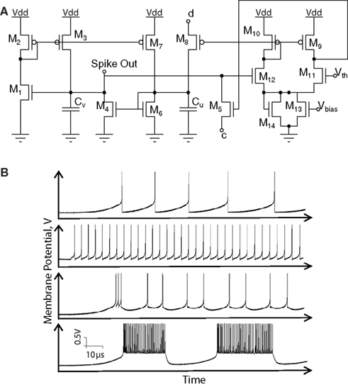
Hardware implementations of spiking neurons are highly beneficial for various applications, including high-speed modeling of large-scale neural systems, real-time operating systems, and bidirectional brain-machine interfaces. The specific circuit solutions for silicon neurons are dictated by the requirements of each...
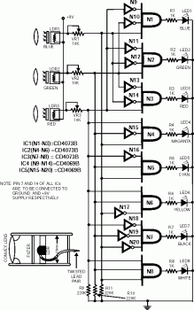
This circuit illustrates a color sensor circuit diagram. The design is grounded in the principles of optics and digital electronics. The color sensor circuit typically employs a light-sensitive component, such as a photodiode or phototransistor, to detect and differentiate colors...
Adrian Bontenbal has provided updated notes from his experiments in recreating Clara Rockmore's theremin. Bob Moog shared his hand-drawn schematic for Clara's instrument over a decade ago. Adrian started with that schematic to build his own Rockmore theremin. During...
The double-limit temperature alarm circuit consists of a temperature detection control circuit, a temperature indicating circuit, and an alarm sound circuit. The components selected include resistors R1 to R5, which should be 1/4W metal film or carbon film resistors....