
TV video output for the EB675001DIP
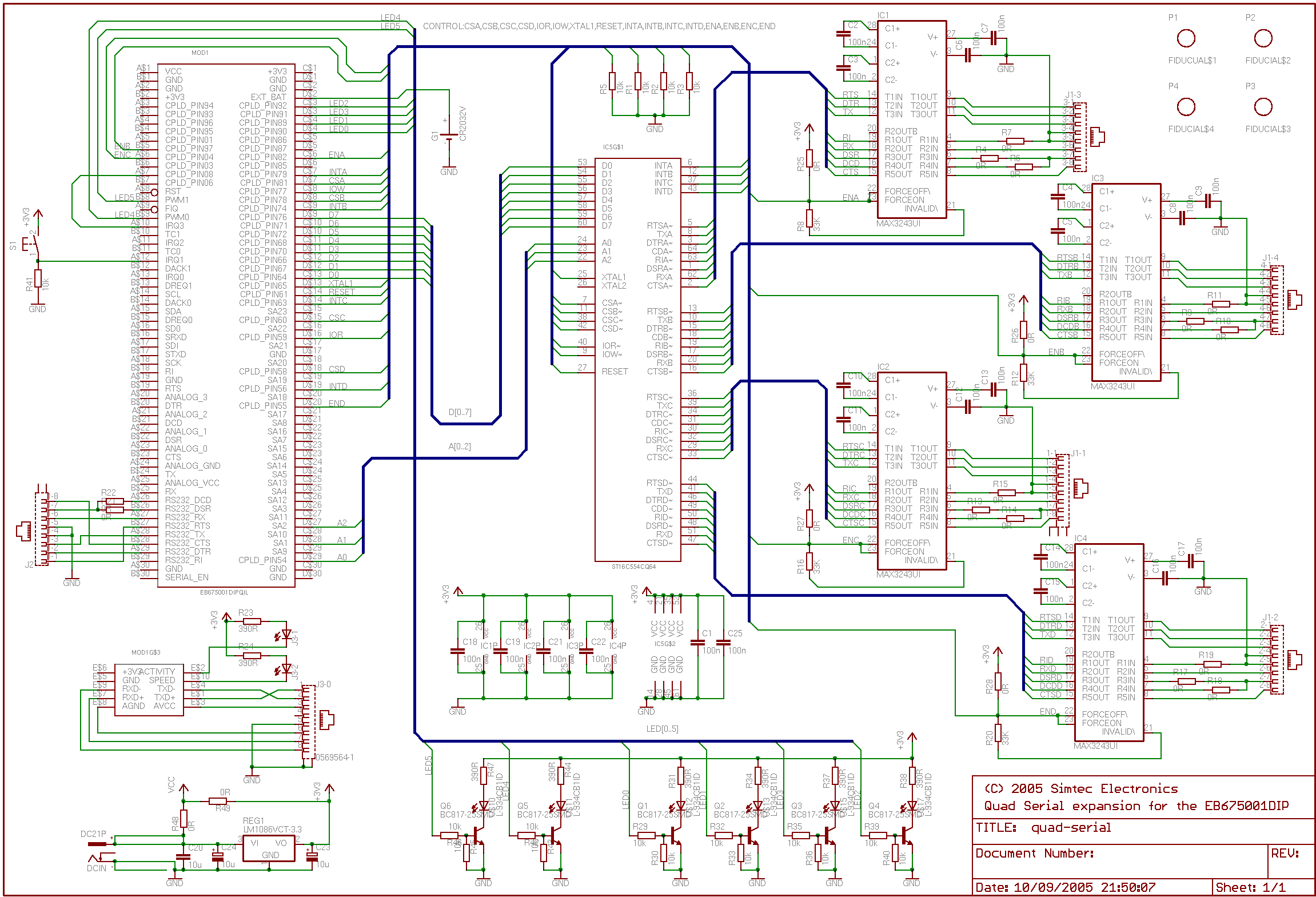
The design of the framebuffer system is a sophisticated integration of various electronic components and logic functions aimed at generating a composite video output suitable for PAL television systems. The use of a CPLD for control and timing logic is particularly advantageous as it minimizes the need for discrete components, thereby reducing overall circuit complexity and improving reliability. The implementation of an external SRAM for framebuffer storage allows for efficient data handling and retrieval, essential for maintaining the required frame rates and synchronization in video output.
The choice of a 256Kbit SRAM is optimal for this application, as it provides sufficient capacity for storing the framebuffer data for multiple scan lines while ensuring quick access times. The timing control generated by the CPLD is critical; it ensures that data is clocked into the shift register at the correct intervals, maintaining the integrity of the video signal. The design's approach to generating SYNC and BLANK signals is also noteworthy, as these signals are crucial for proper display synchronization and image stability.
Moreover, the potential for integrating a light pen functionality through the use of a photodiode introduces an interactive element to the design, enhancing its versatility. This feature allows for user interaction with the display, which can be particularly useful in applications requiring graphical input.
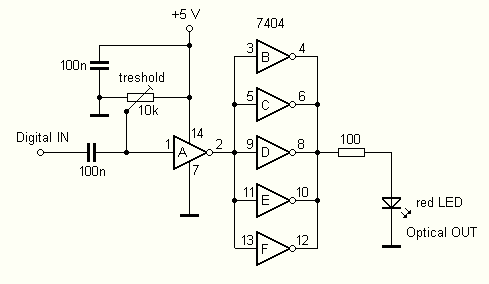
Overall, the described design represents a well-thought-out approach to generating a monochrome composite video output, balancing simplicity with functionality, and providing a foundation for further enhancements or modifications as needed.This application note describes creating a dumb framebuffer with PAL composite TV output for the EB675001DIP. The design uses a minimal number of additional components to achieve this display. The user CPLD is used to provide all control and timing logic reducing circuit complexity. More in depth information on composite video, associated circui ts and techniques can be found across the web a useful resource is the epanorama list of links and Rickard GunG©e video howto Monochrome composite video can be generated with a very simple method. By using two logic outputs and carefully selected resistor values the required voltage levels can be generated.
Composite video in its most basic form consists of a voltage level between 0 and 1V, where 0 V is used for synchronization, 0. 3V is used as black level and 1V is used as a white level. Obviously almost any shade can be created by varying the voltage between the 0. 3 and 1V levels, however for the simple display presented here black and white will suffice. A video frame is made up from two fields of 312 scan lines displayed 25 times a second. For our purposes we will treat the odd and even fields as identical, this halves our vertical resolution but makes the design much simpler as we don`t have to do interlacing, effectively therefore we are producing 312 scan lines 50 times a second giving a line rate of 15, 600 lines per second (strictly speaking each frame has an additional line and the correct line rate is 15, 625 however the missing 25 lines will not prove problematic in practice).
Each scan line lasts for 64 S and consists of a "front porch" of 2 S, a horizontal sync pulse of 4 S, a rear porch of 6 S and 52 S of displayed data. The diagram illustrates this along with a typical scan line waveform for some video bars. The last part of the signal that needs explaining is the vertical synchronization that starts each field, the required waveform is shown in the diagram.
Strictly speaking the second field of each frame should be a slightly different waveform, however in practice this doesn`t seem necessary. The proposed solution uses an external SRAM to hold the framebuffer data. The CPLD is used to generate appropriate timing to clock eight bits from the SRAM into the shift register every 500nS.
A 256Kbit SRAM when clocked in this manner provides 256 64uS scan lines. The shift register is clocked once every 62. 5nS (16MHz rate) giving 1024bits per line, some of these bits will not be viewable as they are output during the boarders and sync times but a continuous clock greatly simplifies the design. In addition to the SRAM clocking the CPLD generates the SYNC and BLANK signals to ensure the output waveform has sync and black levels at the appropriate times.
The CPLD also generates the vertical synchronization waveform and ensures the top and bottom borders are black level. Data is written to the SRAM directly by the OKI CPU, the CPLD ensures correct timing and operation by using the CPU I/O wait function to delay access until the appropriate time.
Because the CPLD generates the vertical sync and can generate an interrupt it is possible to use a photodiode to detect the passing of the scanning beam (on a CRT) and calculate the time elapsed and hence the location of the photodiode on the screen. This would give a light pen function. The schematic creates a specific design from the general ideas outlined previously. The design was generated directly by creating data, address and control buses and connecting the SRAM accordingly.
Initially it was hoped the external shift register could be avoided by integrating it into the CPLD code, however CPLD resources were exhausted and this could not be achieved. The option was left for this mode of operation by adding R3 to the design to allow the CPLD CLK register to be used as the output instead.
The output from the shift register is combined with the SYNC and BLANK signals to all 🔗 External reference
Related Circuits
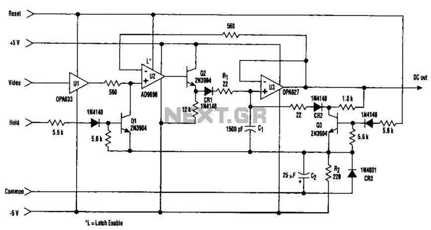
The amplitude of a video signal can be measured using a straightforward circuit that functions as a modified standard peak detector. This device is capable of verifying RGB signals produced by video RAMDACs. U1 is a high-speed buffer, while...
This circuit sequentially lights ten bulbs, first in one direction and then in the opposite direction, creating an appealing visual effect. Gates N1 and N2 form an oscillator, which serves as a clock for the BCD up/down counter CD4510...
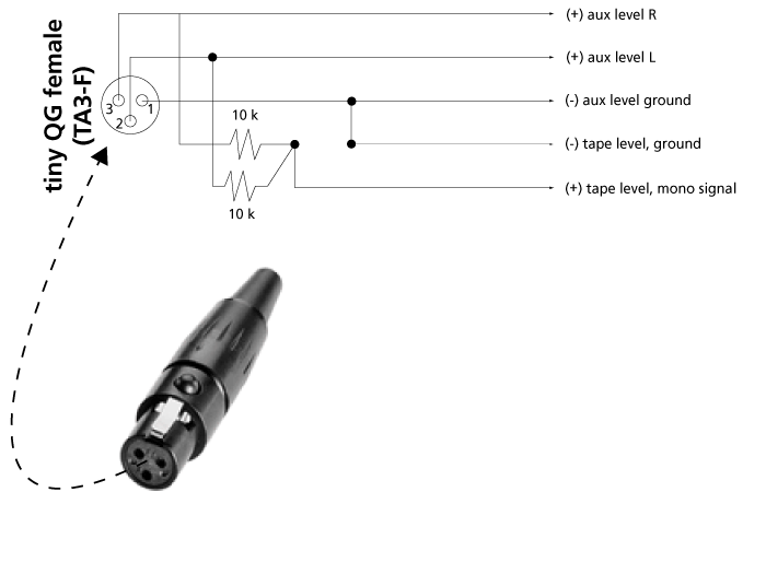
The addition of a mono microphone-level output to the 302 is a beneficial enhancement for connecting transcription recorders, Comtek transmitters, and other inputs. The accompanying diagram demonstrates the correct wiring to create a mono microphone-level output from the tape...
Many modern audio recorders are now compatible with digital input S/PDIF (Sony/Philips Digital Interface). Devices like CD changers, MiniDisc recorders, computer sound cards, and the like work with digital signals using the S/PDIF protocol. This digital connection between two...
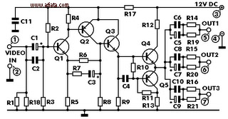
This electronic circuit is a video signal amplifier that provides a broad bandwidth amplifier with a capacity of 5 MHz. It is designed to take video signals from a VCR and amplify them adequately to drive up to three...
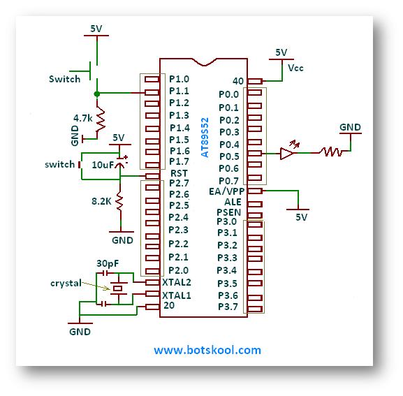
This tutorial continues the discussion on 8051 Assembly Programming by teaching input and output instructions for 8051 microcontrollers using assembly language. The microcontroller comprises a total of forty pins, most of which serve multiple functions. The primary function is...