
ULINKpro Interface Schematic

The schematic represents the interconnections and functionalities of the JTAG (Joint Test Action Group), Serial Wire Debug (SWD), and Embedded Trace Macrocell (ETM) interfaces, which are essential for debugging and programming ARM-based microcontrollers.
The JTAG interface provides a standard method for accessing the debugging features of a microcontroller, allowing for boundary scan testing and in-system programming. It typically consists of a series of pins, including TCK (Test Clock), TMS (Test Mode Select), TDI (Test Data In), and TDO (Test Data Out), facilitating communication between the debugger and the target device.
The Serial Wire Debug interface is a more efficient alternative to JTAG, utilizing fewer pins while maintaining robust debugging capabilities. It employs a two-wire protocol, consisting of SWDIO (Serial Wire Debug Input/Output) and SWCLK (Serial Wire Clock), allowing for a simpler connection to the target hardware.
The Embedded Trace Macrocell interface is designed for real-time tracing of program execution, enabling developers to gather performance metrics and analyze code behavior without significantly impacting system performance. This interface provides a means to capture data such as instruction execution and data accesses.
Overall, the schematic serves as a vital tool for engineers to troubleshoot and optimize the performance of ARM-based systems, ensuring that the necessary interfaces are correctly implemented and functioning as intended.This interface schematic shows the JTAG, Serial Wire, and ETM interface circuits of ULINKpro. Use this schematic to analyze potential problems with the target hardware. ARM websites use two types of cookie: (1) those that enable the site to function and perform as required; and (2) analytical cookies which anonymously track visitors only while usi ng the site. If you are not happy with this use of these cookies please review our Privacy Policy to learn how they can be disabled. By disabling cookies some features of the site will not work. 🔗 External reference
Related Circuits
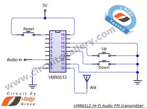
This article provides the circuit schematics for an FM transmitter along with the necessary explanations. The primary component utilized is the VMR6512 IC, a highly integrated FM audio signal transmitter chip designed for Hi-Fi audio applications. This chip can...
A Nidec TA450DC B35502-35 fan has been installed in a large wooden cabinet housing a computer and other electronics, which generates significant heat. The fan is designed to draw air from the room and exhaust it through openings at...
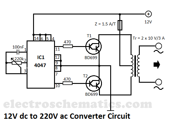
This DIY 12V to 220V voltage converter is built with the CMOS 4047, which serves as the main component of this compact voltage converter that transforms 12V DC into 220V AC. The 4047 is configured as an astable multivibrator,...
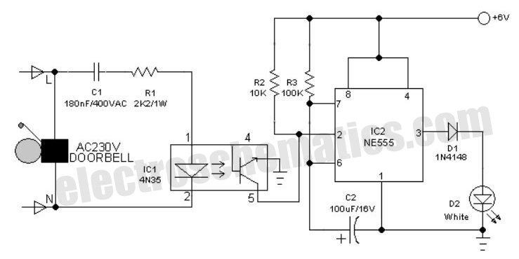
An interesting hobby circuit of a crank doorbell. The circuit is built around a 555 timer and a musical piezo buzzer. It operates using a 9-volt battery supply; a single 9-volt PP3/6F22 compact battery is sufficient to power the...
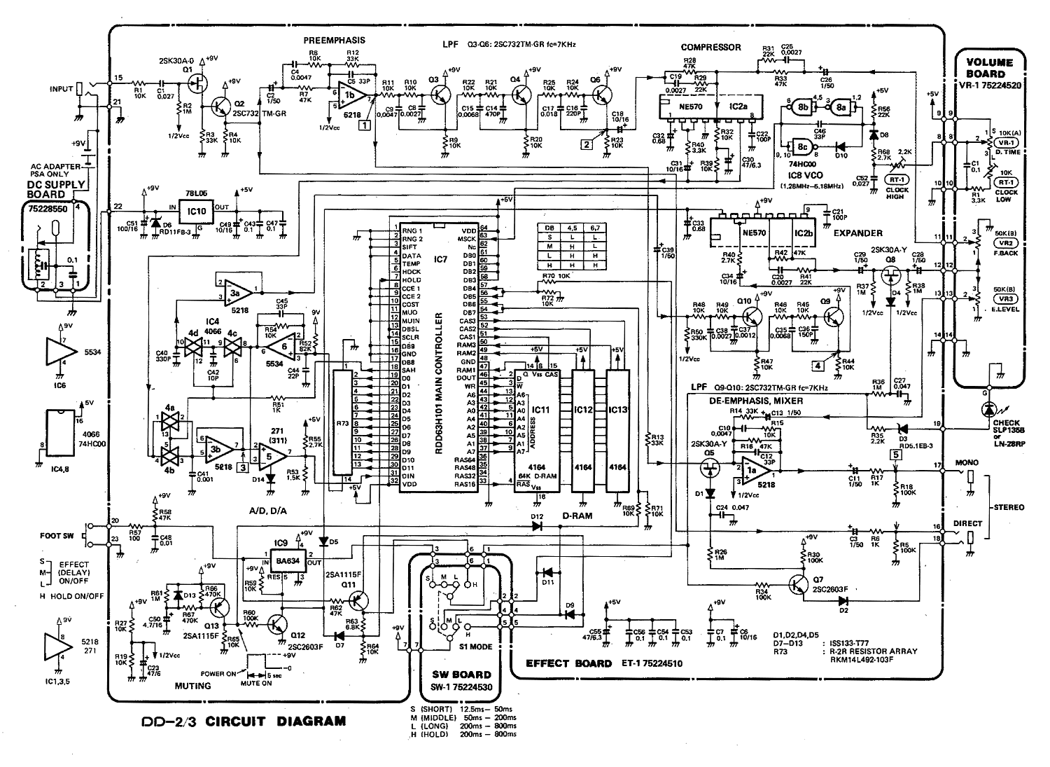
The DD-2 is a highly regarded digital delay pedal that emulates an analog sound. It was initially sold from 1983 until it was discontinued in 1986, after which it was relaunched without any modifications as the DD-3 (noting that...
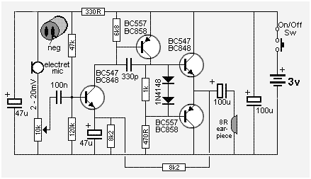
The following circuit presents a Mini Audio Amplifier Circuit Schematic Diagram. Features include a power consumption of less than 3mA, a small output, and the use of a push-pull configuration. The Mini Audio Amplifier Circuit is designed to amplify low-level...