
Understand Radio Architectures
The RF front end comprises several critical components that work in concert to ensure effective signal reception and processing. The antenna is designed to capture the desired radio waves, and its characteristics must be matched to the frequency of interest to optimize performance. The RF filter plays a crucial role in eliminating unwanted signals and noise, ensuring that only the desired frequency components are passed to the next stage.
In the case of the AM detector receiver, the detector diode's role cannot be understated. It rectifies the incoming RF signal, allowing the audio information to be extracted. The choice of diode, whether a traditional point-contact type or a more modern pn-junction diode, affects the performance and reliability of the receiver. The configuration of the circuit, including the placement of inductors and capacitors, is essential for tuning the receiver to the desired frequency and ensuring effective demodulation.
Furthermore, the design of the PCB is paramount in minimizing losses and ensuring that the RF signals are transmitted with minimal degradation. The layout must consider aspects such as trace width, ground planes, and component placement to optimize signal integrity and reduce potential interference.
Overall, the design of an RF front end is a complex task that requires careful consideration of various factors, including the type of modulation, the frequency of operation, and the specific application requirements. As technology continues to evolve, advancements in materials and component design will further enhance the performance of RF front ends, making them more efficient and capable of handling increasingly complex signals.The fundamental operation of an RF front end is fairly straightforward: it detects and processes radio waves that have been transmitted with a specific known frequency or range of frequencies and known modulation format. The modulation carries the information of interest, be it voice, audio, data, or video. The receiver must be tuned to resonate w ith the transmitted frequency or frequencies in order to detect them. Those received signals are then filtered from all surrounding signals and noise and amplified prior to a process known as demodulation, which removes the desired information from the radio waves that carried it. These three steps ”filtering, amplification and demodulation ”detail the overall process. But actual implementation of this process (i. e. , designing the physical RF receiver printed-circuit board (PCB) depends upon the type, complexity, and quantity of the data being transmitted.
For example, designing an RF front end to handle a simple amplitude-modulated (AM) signal requires far less effort and hardware (and even software) than building an RF front end for the latest third-generation (3G) mobile telecommunications handset. Because of the enhanced performance of analog components due to IC process improvements and decreasing costs of more powerful digital-signal-processing (DSP) hardware and software functions, the ways that different RF front-end architectures are realized has changed over the years.
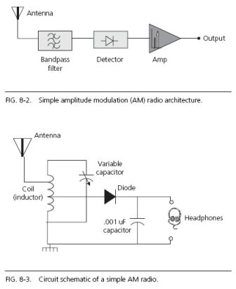
Still, the basic requirements for an RF front end, such as the frequency range and type of carrier to be received, the RF link budget, and the power, performance, and size restrictions of the front-end design, remain relatively the same in spite of the differences in radio architectures. One of the basic RF receiver architectures for detecting a modulated signal is the amplitude modulation (AM) detector receiver (see Fig.
8-2). The name comes from the fact that information like speech and music could be converted into amplitude (voltage) modulated signals riding on a carrier wave. Such an RF signal could be de-modulated at the receiving end by means of a simplediode detector. All that is needed for a basic AM receiver ”like a simple crystal radio ”is an antenna, RF filter, detector, and (optional) amplifier to boost the recovered information to a level suitable for a listening device, such as a speaker or headphones.
The antenna, which is capacitive at the low frequencies used for AM broadcasting, is series matched with an inductor to maximize current through both, thus maximizing the voltage across the secondary coil. A variable capacitance filter may be used to select the designed frequency band (or channel) and to block any unwanted signals, such as noise.
The filtered signal is then converted to demodulate the AM signal and recover the information. Fig. 8-3 represents a schematic version of the block diagram shown in Fig. 8-2. The heart of the AM architecture is the detector demodulator. In early crystal radios, the detector was simply a fine metal wire that contacted a crystal of galena (lead sulfide), thus creating a point contact rectifier or crystal detector. In these early designs, the fine metal contact was often referred to as a catwhisker. Although point-contact diodes are still in use today in communication receivers and radar, most have been replaced by pn-junction diodes, which are more reliable and easier to manufacture.
For a simpleAM receiver, the detector diode acts as a half-wave rectifier to convert or rectify a received AC signal to a DC signal by blocking the negative or positive portion of thewaveform (see Fig. 8-4). A half-wave rectifier clips the input signal by allowing either the positive or negative half of theAC wave to pass easily through the rectifier, depending upon the polarity of the rectifier.
A shunt inductor is typically placed in front of the detector to serve as an RF choke. The inductor maintains the 🔗 External reference
Related Circuits
As packet radio began to gain popularity, the limitations of the initial experience with the "BSX1" TNC became apparent. It only supported AX25 version 1 and had restricted input/output capabilities. Additionally, the command set was not standardized, diverging from...
The recommendation regarding the existing phono connector is to maintain its current configuration without making significant alterations. The procedure involves replacing the electrolytic and paper capacitors, adding a three-wire line cord, and utilizing the radio in its original state....
The CXA1619BM and CXA1619BS are one-chip FM/AM radio integrated circuits developed by Sony Corporation. These ICs are intended for use in radio-cassette tape recorders and headphone tape recorders, offering a variety of functions. The CXA1619BM and CXA1619BS are designed to...
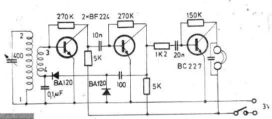
Oscillating circuits (coils) are constructed on a ferrite bar. For long wave reception, winding "1-2" consists of 135 turns, while winding "3-4" consists of 20 turns. For medium wave reception, winding "1-2" has 75 turns, and winding "3-4" has...
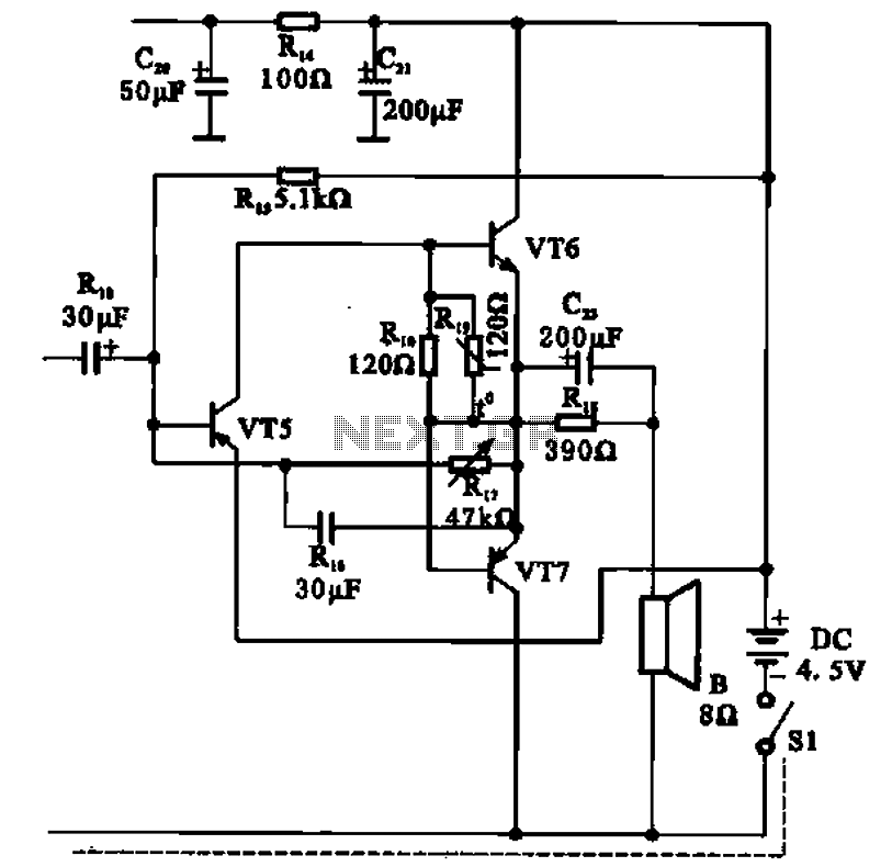
The transistor radio features a common output transformerless (OTL) power amplifier circuit. The VT5 component serves as the bias resistor for the driver stage. VT6 and VT7 form a complementary symmetry configuration, with VT6 being a germanium NPN transistor...
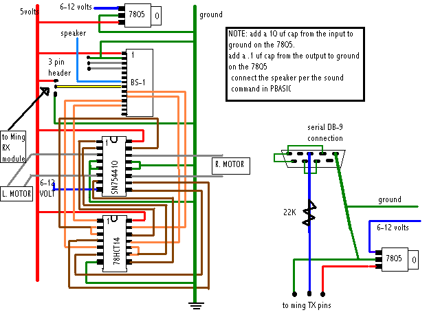
This project allows for the control of two wheels or tracks from a PC serial port without any wired connections. The system operates at 2400 baud. A Basic Stamp microcontroller is utilized, with the Basic Stamp I being used...