
Universal adder 741 1458 schematic
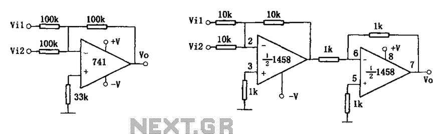
The inverting adder circuit is a fundamental operational amplifier (op-amp) configuration used to perform the addition of multiple input signals. In this configuration, the op-amp is connected in an inverting mode, where the inputs are applied through resistors to the inverting terminal. The non-inverting terminal is typically grounded.
In the inverting adder circuit (Figure a), the output voltage (Vo) is a negative sum of the input voltages (Vi1 and Vi2), scaled by the feedback and input resistors. The relationship can be mathematically expressed as Vo = - (Vi1 + Vi2), indicating that the output is inverted relative to the sum of the inputs. The resistors connected to the input terminals determine the gain of each input signal. If the resistors are equal, the outputs will be inversely proportional to the inputs.
For phase addition, the circuit depicted in Figure (b) employs a different configuration that allows for the summation of input signals without inversion. In this case, the output voltage is given by Vo = (Vi1 + Vi2), which directly represents the algebraic sum of the input voltages. This configuration typically involves a non-inverting summation approach, where the op-amp is configured to add the inputs in phase, resulting in a positive output that reflects the total of the input signals.
Both configurations are widely used in analog signal processing applications, such as audio mixing, data acquisition systems, and various forms of signal manipulation where the summation of multiple signals is required. Proper selection of resistor values and op-amp specifications is crucial to ensure desired performance, including bandwidth, slew rate, and output drive capability. As shown for the common addition circuit. Figure (a) is the inverting adder circuit, an input-output relationship is: Vo - (Vil + Vi2) When you need to phase addition, the circ uit shown in Figure may be used (b), the input-output relationship is: Vo Vil + Vi2
Related Circuits
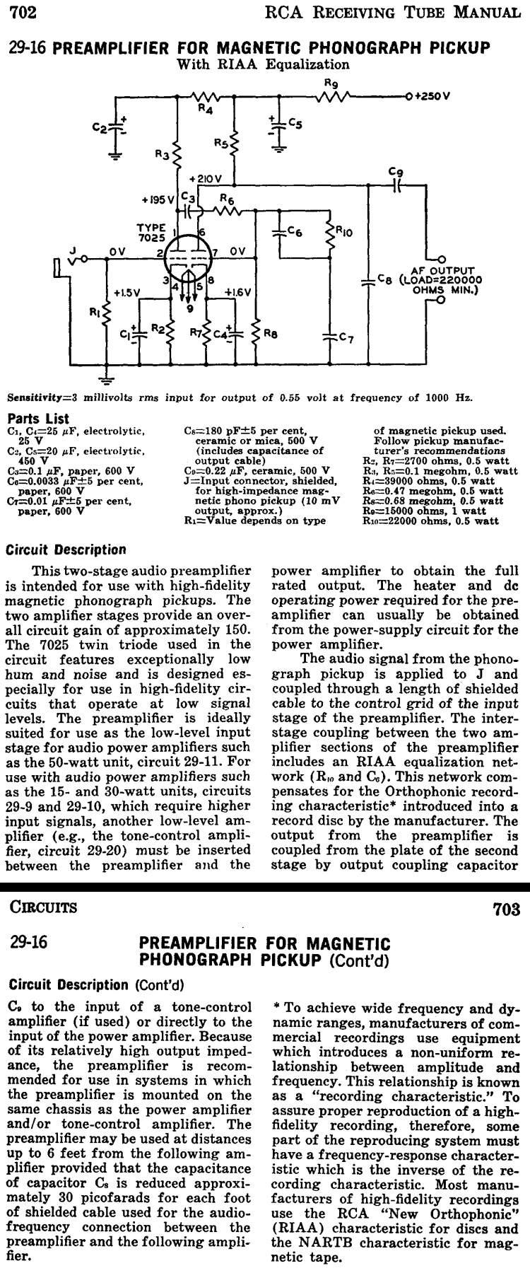
This two-stage audio preamplifier is designed for high-fidelity magnetic phonograph pickups, providing an overall gain of approximately 150. The circuit is sourced from the RCA tube receiving manual and is intended for use with the renowned RCA 7025 twin...
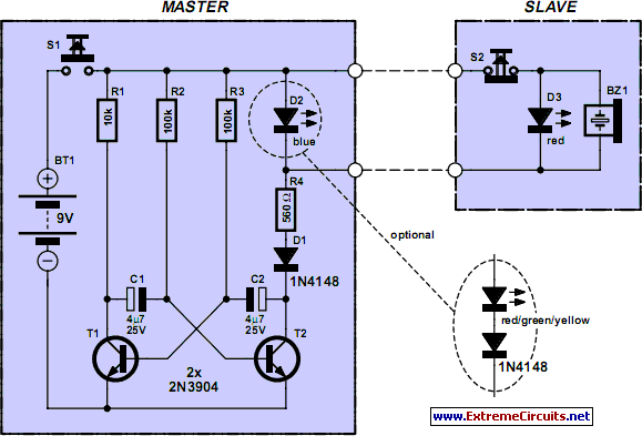
This circuit can be utilized by individuals, such as a gentleman summoning his butler, a manager calling for his secretary, or, as in the author's case, to call children down for dinner without raising one's voice over the noise...

Often the need to control light switch on the instrument. If napájíme LED source of low DC voltage sufficient to classify a series of LED-resistor of appropriate resistance. Another situation occurs, if a small supply available, or to indicate...
The car power amplifier utilizes the SI1050GL integrated circuit (IC) as the primary amplification component. It delivers an output power of 50 Watts at an 8-ohm mono impedance. The amplifier operates with a DC voltage of up to 25...
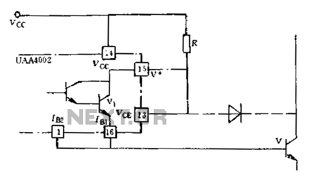
Anti-saturation devices have been removed from the UAA4002 routine applications. The base current of the switching transistor, which is driven by another transistor, is automatically adjusted. This adjustment allows the power transistors to operate in critical saturation. However, when...
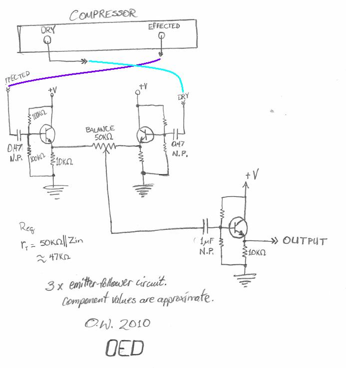
A simple wet/dry knob is desired to be added to a GSSL (Chameleon Labs 7720) for parallel compression. A relevant schematic has been found. To implement a wet/dry knob for parallel compression on a GSSL (Chameleon Labs 7720), the circuit...