
Universal Laboratory Power Supply Circuit
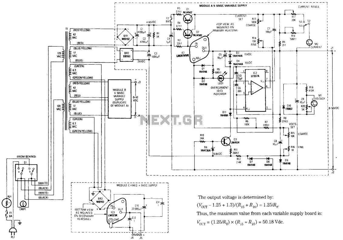
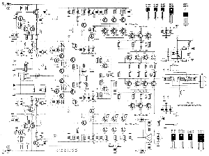
The circuit utilizes an LM317HVK voltage regulator, known for its versatility in providing adjustable output voltages and robust current-limiting capabilities. This component is essential for applications requiring a stable voltage supply over a wide range of input voltages. The input stage, represented by BR1, functions as a bridge rectifier, converting alternating current (AC) to direct current (DC). The filtering capacitors, C1 and C2, play a critical role in smoothing the rectified output, ensuring that the voltage presented to the LM317HVK is stable and within the operational limits.
The current-sense comparator IC2 is an integral part of the circuit, designed to monitor the output current and provide feedback for regulation purposes. The input from BR2 facilitates the generation of a negative bias voltage, which is crucial for certain configurations of the LM317HVK, particularly in applications where the output voltage needs to be regulated down to ground potential. This negative bias allows for enhanced control over the output voltage, ensuring that the system can maintain desired performance levels even under varying load conditions.
Overall, the combination of these components enables the design to achieve reliable voltage regulation and current limiting, making it suitable for various electronic applications where power management is critical. The value of the design lies in the use of IC1, an LM317HVK adjustable s.eries-pass voltage regulator, for broad-range performance remainder supplies voltage-setting and current-limiting functions. The input to ICI-comes from the output of BR1, which is filtered by CI and C2 to about +60 Vdc, and the input for current-sense comparator IC2 comes from BR2,
which also acts as a negative bias supply for regulation down to ground. 🔗 External reference
Related Circuits
Section Ul-a is configured as a high-gain inverting voltage amplifier that is inductively coupled to the phone line via LI. Inductor LI is a homemade unit that consists of 250 turns of fine, enamel-coated wire that is wound on...
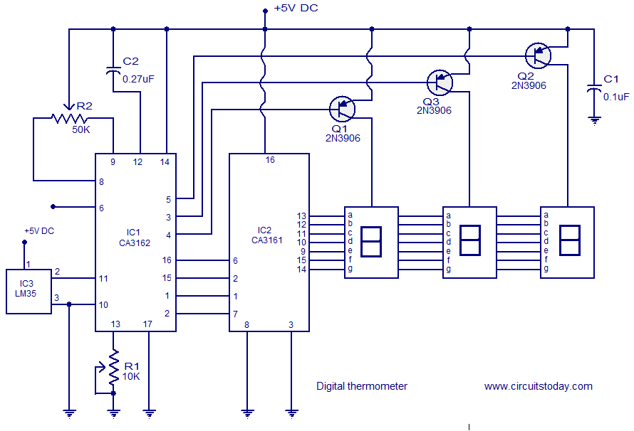
A simple digital thermometer circuit without a microcontroller and featuring a seven-segment LED readout is presented. The circuit utilizes three integrated circuits (ICs): CA3162, CA3161, and LM35. The CA3162 is a monolithic analog-to-digital (A/D) converter with a BCD output....
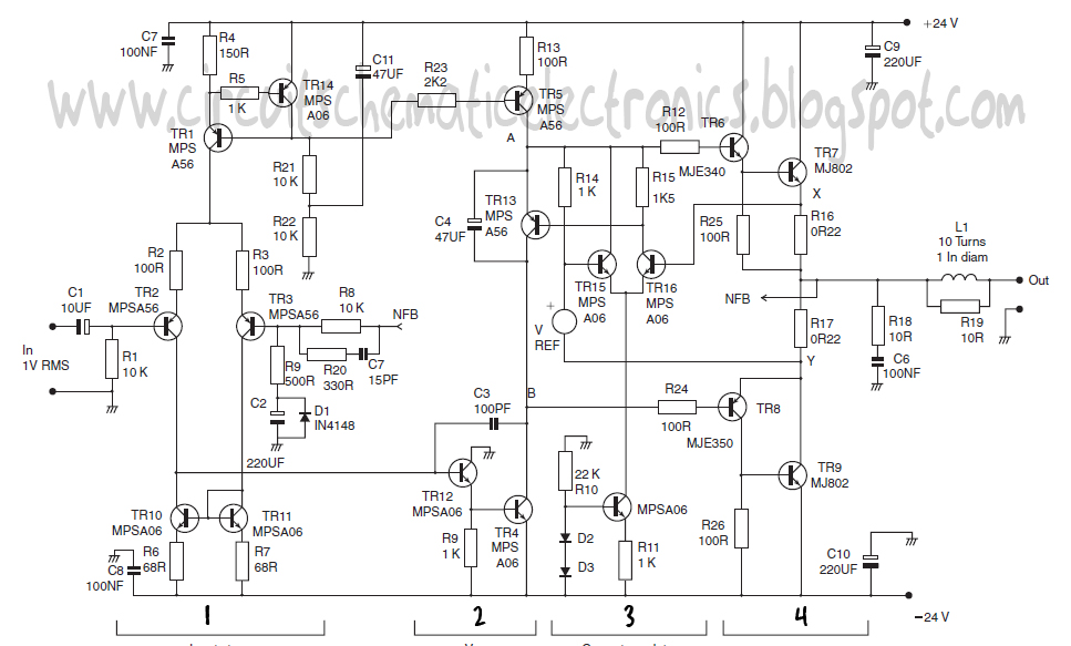
This design schematic represents a Class A power amplifier. It closely matches the operating parameters of Class B to facilitate comparison, particularly with a negative feedback (NFB) factor of 30dB at 20 kHz. The front end is similar to...
The following circuit illustrates a 2000W Power Amplifier Circuit Diagram. This circuit utilizes the BC560C transistor. Features include a robust design. The 2000W power amplifier circuit is designed to deliver high output power suitable for various applications, including audio amplification...
The following circuit illustrates a Cat and Dog Repellent Timer Circuit Diagram. Features include the capability to maintain a deep cycle battery charged by a solar panel. The Cat and Dog Repellent Timer Circuit is designed to provide a humane...
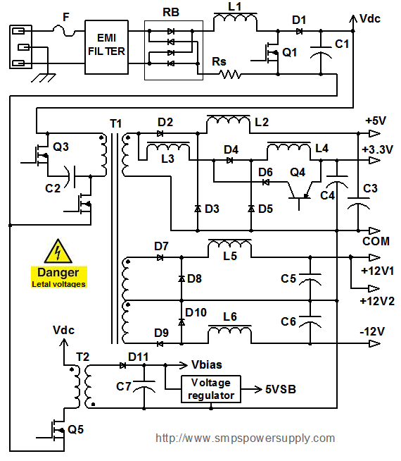
All electronic systems and equipment, regardless of their size or function, share a common requirement: a power supply unit (PSU) that converts input voltage into suitable voltage levels for their circuits. The most prevalent type of PSU today is...