
Ups 5Volt Circuit

The circuit described operates as a dual-regulator system powered by a 9-V wall adapter. The primary function of the low-battery detector circuit integrated into IC2 is to monitor the input voltage (l7IN) using resistors R6 and R7. When the battery voltage falls below a predetermined threshold, the detector activates, sending a signal to pin 7. This output is connected to an inverter (Q1), which serves to control the shutdown inputs of both regulators, IC1 and IC2. The opposite-polarity active levels of these shutdown inputs ensure that only one regulator operates at a time, thus optimizing power consumption.
The feedback resistors R2 and R3 are crucial as they allow both IC1 and IC2 to continuously monitor the output voltage (V0VT), ensuring that the output remains stable and within the desired voltage range. In the event that IC2 detects an out-of-spec condition and shuts down, it effectively turns off its output, preventing any further power draw from the adapter.
In scenarios where IC1 shuts down, the entire circuit enters a low-power state, significantly reducing the current draw to below 1 mA, which is essential for battery-powered applications where efficiency is critical. The components LI, D2, Q1, C2, R2, and R3 are integral to the operation of the 250-mW switching regulator, providing the necessary voltage regulation and stability.
Diodes D3 and D4 are configured in a wire-OR arrangement to ensure that power is reliably supplied to IC2, enhancing the redundancy of the power supply. Additionally, Q3 plays a vital role in improving the load regulation of the linear regulator, ensuring that the output voltage remains consistent under varying load conditions. This comprehensive design ensures robust performance and efficiency in power management applications. A 9-V wall adapter supplies Vm. IC2 contains a low-battery detector circuit that senses l7IN by means of R6 and R7. The detector output Cpin 7) drives an inverter (Ql), which in turn drives the shut-down inputs Ic of 1C1 and SHDN of IC2. These inputs have opposite-polarity active levels. The common feedback resistors, R2 and R3 enable both regulators to sense the output voltage, V0VT. When IC2 shuts down, its output turns off. However, when IC1 shuts down, the whole chip assumes a low-power state and draws under 1 . LI, D2, Gl, C2, R2, and R3 are part of the 250-mW switching regulator. Diodes D3 and D4 wire-OR the power connection to IC2, and 03 improves the linear regulator`s load regulation.
Related Circuits
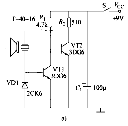
The ultrasonic transmitter circuit T-40-16, along with various discrete components, functions as a feedback sensor. The transistors VT1 and VT2 create a robust positive feedback oscillator that converts an electric signal into an ultrasonic oscillation signal, with the oscillation...
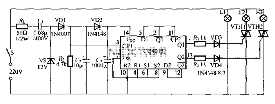
Figure 296 illustrates a control circuit that utilizes a switch (S) to manage three lamps (E1, E2, and E3) in a lighting system, suitable for controlling a chandelier in a living room. When the switch is off, all lights...
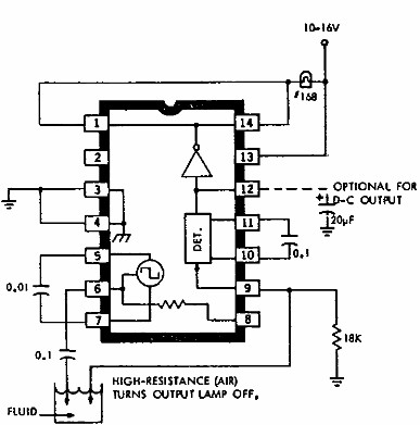
This electronic liquid detector circuit diagram utilizes the ULN2429A monolithic bipolar integrated circuit, which is designed to detect the presence or absence of various types of liquids. The detection mechanism involves comparing the resistance of a probe immersed in...
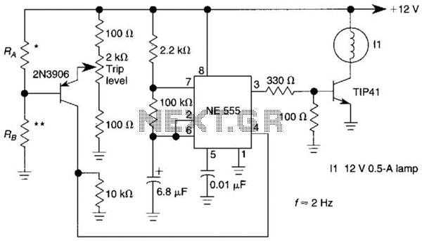
A sensor activates transistor Q1 to turn on the low-frequency 555 oscillator, which generates pulses to control LAMP II. The sensor may respond to variations in light or temperature. Either resistor RA or RB can function as the sensor,...
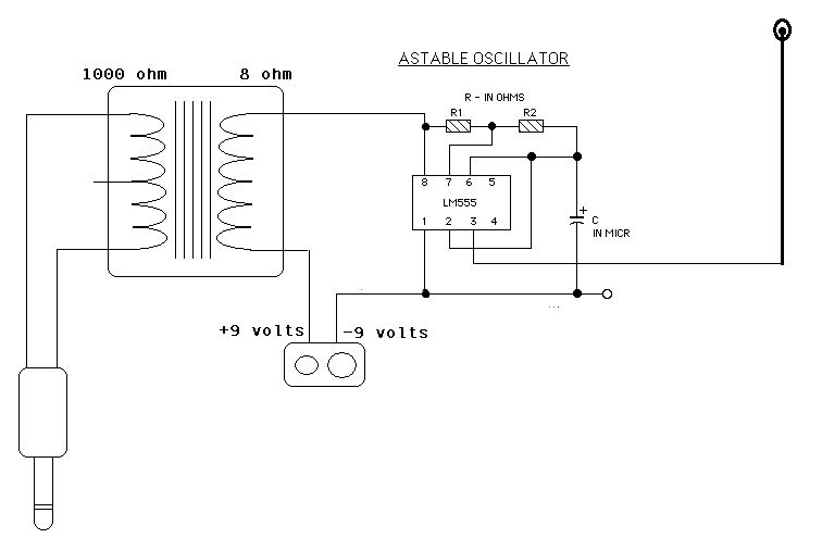
Two ICM7555 CMOS 555 timers are available, and there is an inquiry about effective AM radio transmitter circuits that utilize one or both of these timers. The ICM7555 is a low-power CMOS version of the classic 555 timer, which can...
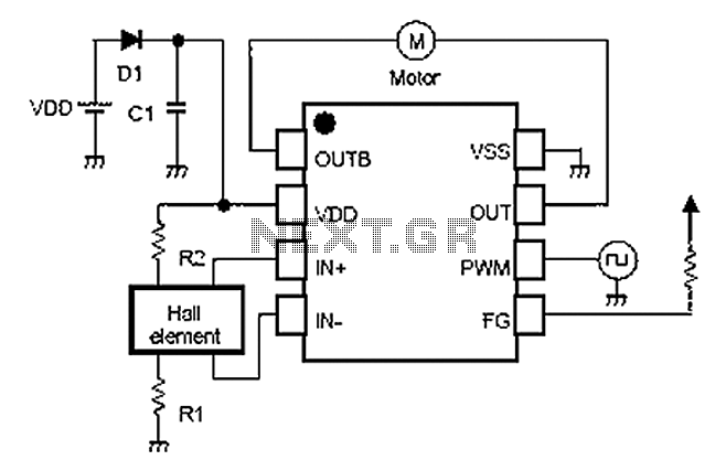
A simple single-phase brushless DC motor drive using the NJU7365 motor driver IC from New Japan Radio Co., Ltd. The NJU7365 is designed for single-phase motor applications and features built-in MOSFET motor drives, direct PWM input, FG output, and...