
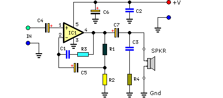
Use upC1663 broadband amplifier
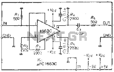
The PCI663 integrated circuit functions primarily as a differential amplifier, designed to convert a differential input signal into a single-ended output while maintaining high fidelity. The circuit topology employs a resistor network to balance the input and output stages, ensuring that the signal integrity is preserved.
The terminal resistance of 50 ohms is critical for impedance matching, minimizing reflections and maximizing power transfer in high-frequency applications. The use of straight coupling further enhances signal transmission by reducing potential losses associated with more complex coupling methods.
The output voltage being in phase at approximately 3V indicates that the circuit is optimized for applications requiring a stable output reference. The inclusion of a coupling capacitor is essential for AC applications, as it blocks any DC offset that may be present in the signal, allowing only the AC component to pass through.
In configurations where single-ended outputs are utilized with differential terminals, maintaining circuit stability is crucial. The introduction of a balancing resistor mitigates the risks associated with open-circuit conditions, which can lead to unpredictable behavior and distortion of the output signal.
The gain characteristics of the circuit are adjustable through the selection of the emitter resistor, Rs. The noted gains of 300 times and 100 times at specific load conditions illustrate the circuit's flexibility in amplification. The ability to incorporate a variable resistor allows for fine-tuning of the gain, which is particularly advantageous in applications requiring precise signal amplification.
Overall, this circuit design demonstrates a high level of performance, offering superior frequency characteristics compared to traditional operational amplifiers. This makes it suitable for a variety of applications in signal processing, where both gain control and signal integrity are paramount.j1PCI663 shame dynamic is input, differential output type of IC, but this circuit has a single-ended output, input terminal resistance chu l (50Q), comb straight coupling. Because the output voltage is approximately the same phase 3V, it is necessary to use a capacitor c: aiE line AC coupling. When using single-ended output differential output terminals If not using open-circuit, the characteristics will change, so this circuit is connected to the resistance fart 'ugly chu, in order to achieve balance.
Magnification is connected by a differential input differential transistor emitter resistor Rs. OK, short circuit, which is about 300 times when looQ}} 1.2kQ 100 times when 20 times. If lkQ variable resistor, you can arbitrarily change the magnification. That is the change to the closed-loop magnification, it will not change the frequency characteristics of the circuit which is superior to ordinary OP amplifier place.
Related Circuits
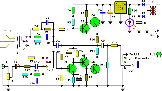
The described shunt-feedback configuration facilitates the straightforward incorporation of frequency-dependent networks, enabling a practical and unobtrusive switchable tilt control as an optional feature. When switch SW1 is in the first position, a gentle shelving bass boost and treble cut...
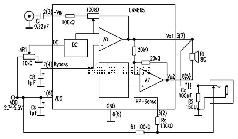
A 750mW bridge-tied load audio amplifier circuit utilizing the LM4065 amplifier is presented below. The LM4865 is available in an 8-pin SO package and an 8-pin mini SMD package. The power supply voltage (VDD) ranges from 2.7V to 5.5V,...
Can be directly connected to CD players, tuners and tape recorders. Simply add a 10K Log potentiometer (dual gang for stereo) and a switch to cope with the various sources you need. Q6 & Q7 must have a small...
This compact amplifier is built around the TDA2003 integrated circuit, which can deliver 4W RMS at a 4-ohm load. The TDA2003 offers enhanced performance while maintaining the same pin configuration as the TDA2002. It retains the advantageous features of...
The closer the two transistors are matched, the better the performance. It is advisable to use TIP41 and TIP42 transistors, which are closely matched NPN and PNP power transistors with a dissipation rating of 65 watts each. If a...
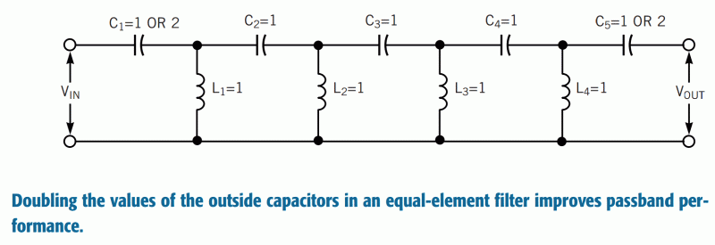
Using a modified equal-element design for a lumped-circuit lowpass filter has several advantages over the well-known equal-element design. The modified design exhibits superior passband performance with only modest degradation of stopband selectivity. Moreover, the modified design is simple and...
Warning: include(partials/cookie-banner.php): Failed to open stream: Permission denied in /var/www/html/nextgr/view-circuit.php on line 713
Warning: include(): Failed opening 'partials/cookie-banner.php' for inclusion (include_path='.:/usr/share/php') in /var/www/html/nextgr/view-circuit.php on line 713