
Variable gain differential amplifier circuit diagram A709
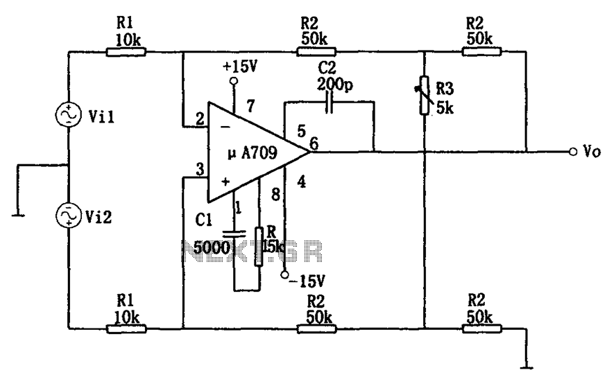
The A709 differential amplifier circuit is designed to provide adjustable gain while maintaining high linearity and stability. By utilizing precision resistors for R1 and R2, the circuit ensures that the differential gain can be finely tuned without compromising the integrity of the signal. The resistive divider formed by R2 and R3 allows for a smooth transition in gain settings, making it suitable for applications requiring variable amplification.
The inclusion of the RC compensation network is essential for stabilizing the amplifier, particularly in high-frequency applications where parasitic capacitance can lead to unwanted oscillations. The choice of capacitor value for C2 is critical; it should be selected based on the desired bandwidth and stability margins of the amplifier. The relationship between the gain and the resistor values can be adjusted to optimize performance for specific applications, such as instrumentation or audio processing.
In practical implementations, attention must be paid to the power supply voltage to avoid saturation of the output. The design should ensure that the amplifier operates within its linear range, and proper decoupling capacitors should be used to minimize power supply noise, which can affect the performance of the circuit.
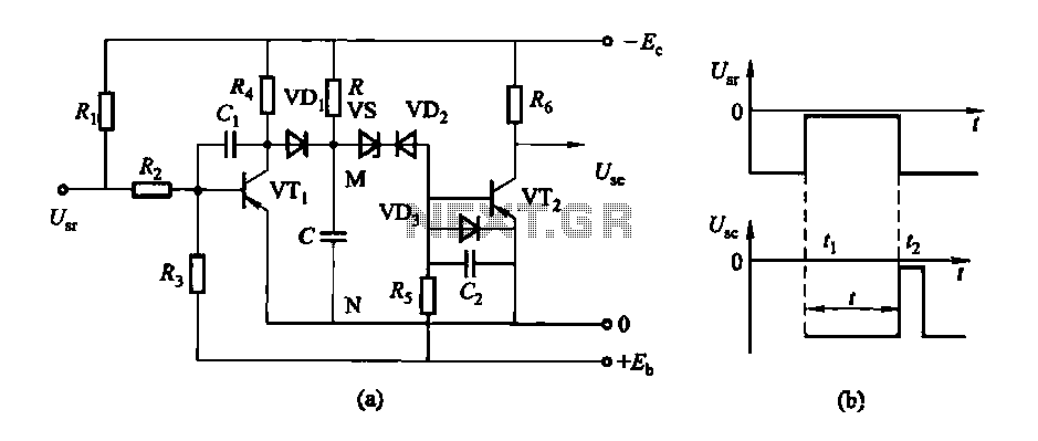
Overall, the A709 differential amplifier circuit stands out for its flexibility and performance, making it a valuable component in a variety of electronic systems where signal conditioning is required. As shown for the configuration of the variable gain A709 differential amplifier circuit. The biggest advantage of the circuit is in keeping CMRR KCMR same premise, continuously adjustable differential gain can be achieved. Circuit four resistors R2 and two resistors R1 resistance must be equal, respectively, the numerical figure shows the typical application time. Adjust potentiometer R3, can realize continuous adjustment voltage magnification. If the adjusted gain adjustment resistor R3 5, the corresponding ratio R2/R3 104, where the voltage amplification Av -104 (2R2/R1), the adjustment range of the apparent gain of the circuit is very wide and easy adjustment.
It needs to be emphasized that: the voltage gain is not too large, because when the gain is large Vo near the power supply voltage, the output voltage will be a serious nonlinear distortion. In addition, the introduction of a RC between pin 1,8 compensation branch, between pins 5 and 6 also introduces a compensation capacitor C2, to improve the stability of the circuit, to prevent parasitic oscillation.
The basic relationship of the circuit is: Vo - (2R2/R1) (1 + R2/R3) (Vi1-Vi2) Av Vo/(Vi1 a Vi2) - (2R2/R1) (1 + R2/R3) When R1 10k, R2 50k, R3 5k when, Av -110. A709 integrated chip electrical parameters (VD 15V, TA 25 )
Related Circuits
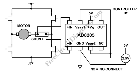
A differential current sensing circuit is integrated within an H-bridge configuration, as illustrated in the schematic diagram below. This circuit exemplifies the application of the AD8205, which is capable of measuring current in both directions as the motor changes...
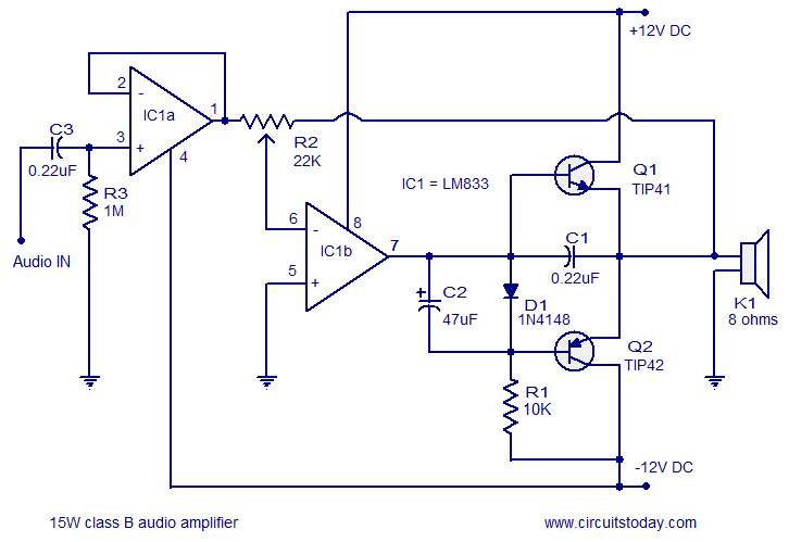
A 15 Watts Class B audio amplifier circuit is designed using a dual op-amp LM833. The schematic diagram is provided, and a potentiometer allows for volume control. The 15 Watts Class B audio amplifier circuit utilizes the LM833 dual operational...
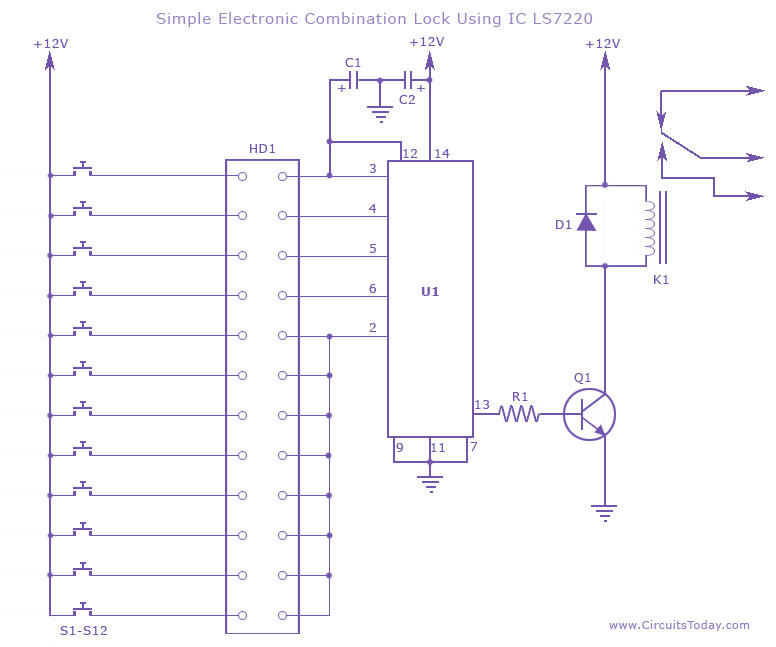
This circuit diagram illustrates a simple electronic combination lock utilizing the IC LS7220. It is designed to activate a relay for controlling any device (on & off) when a specific combination of four digits is entered. The circuit operates...
Clearly indicate on the circuit diagram each type and size of the components. There is a need for assistance in designing a low power FM transmitter circuit, specifically using the BA1404 FM transmitter with a center frequency of 79W...
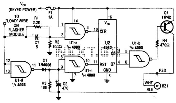
This circuit counts the flashes of turn signals. After approximately 70 flashes, a chime sounds to remind the driver to deactivate the turn signal. The period can be altered by using different taps on U2 if desired. BZ1 serves...
The circuit features a delay action with an instantaneous reset control mechanism. It is categorized into three types: a conducting pipe rechargeable delay circuit, a tube cut-off control rechargeable delay circuit, and a discharge-type delay circuit. In the conducting...