
VFC110: Single Chip High-Frequency Voltage-to-Frequency Converter (VFC)
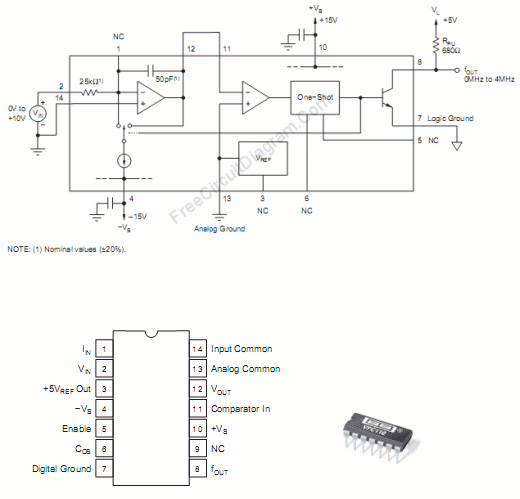
The VFC110 voltage-to-frequency converter is designed to convert an analog voltage input into a frequency output, making it suitable for various applications requiring frequency modulation of voltage signals. The high-frequency capability of the VFC110 enables it to handle input voltages ranging from 0V to 10V, translating this range into a frequency output from 0 Hz to 4 MHz.
The chip's internal architecture includes a precision 5V reference, which is crucial for maintaining accuracy in the conversion process. This reference voltage can be used to calibrate the output frequency, ensuring that the converter operates within specified tolerances. The disable function allows for power management by turning off the chip when not in use, thus reducing power consumption.
The output stage, designed as an open collector, allows for easy interfacing with other digital circuits. This configuration means that the output can be connected to various logic families, including TTL and CMOS, making the VFC110 versatile for integration into different electronic systems.
For the circuit design, the use of a pull-up resistor is essential for ensuring that the output signal is pulled to a high state when the open collector output is not actively driven low. The inclusion of two bypass capacitors is vital for filtering power supply noise, which can adversely affect the performance of the voltage-to-frequency conversion. The recommended 100nF mylar capacitors are effective in providing stable power supply conditions, enhancing the reliability of the converter's output.
Overall, the VFC110 chip represents an efficient solution for converting voltage levels into corresponding frequency signals, suitable for applications in signal processing, sensor interfacing, and data acquisition systems.Using VFC110 chip, we can build a high frequency voltage-to-frequency converter. The features of this chip include the capability of high frequency operation, disable function, and an on-board precision 5V reference. This precision reference can be used to provide reference for offsetting the VFC transfer function, as well as provide transducer or
bridge excitation. As well as shutting off the single VFC chip, Multiplexing several VFC outputs can be done by the enable function. The output is an open collector stage that is compatible with TTL or CMOS logics. Here is the schematic diagram of the circuit: You can see that this circuit only use a pull up resistor for the output and two bypass capacitors for power supply filtering.
You can use a 100nF mylar cap for these two bypassing capacitors. Using minimum the component count, this circuit provide 0-4MHz output for 0-10V input voltage. [Circuit`s schematic diagram source: Texas Instruments Application Notes] 🔗 External reference
Related Circuits
The signals below 550 kHz include maritime mobile, distress signals, radio beacons, aircraft weather information, European Longwave-AM broadcasts, and point-to-point communications. A low-frequency converter transforms the 10 to 500 kHz LW range into a 1010 to 1550 kHz MW...
This article outlines a proposed solution for a 200 W power supply utilizing the FSFR2100 Fairchild Power Switch (FPS). The input voltage range is 90 to 265 VRMS, and it features six outputs. The 200 W power supply circuit based...
This simple battery charger circuit is designed for NiMH/NiCd batteries. It requires no microcontroller or any programming. Linear Technology Corporation. The described battery charger circuit is intended for use with nickel-metal hydride (NiMH) and nickel-cadmium (NiCd) batteries, which are commonly...
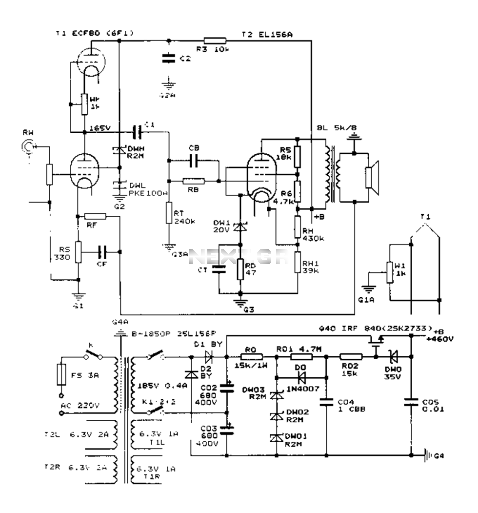
The Danji mellow sound is characterized by its transparent and natural quality, offering a sweet and sincere listening experience that is tireless over long durations and rich in humane color. Tube amplifiers have become an audiophile's companion and are...
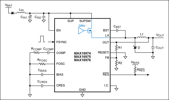
Optimize the layout of the MAX16974/MAX16975/MAX16976 high-performance DC-DC converters, which are standard buck controllers designed for automotive applications. The MAX16974, MAX16975, and MAX16976 are advanced DC-DC buck converters specifically tailored for automotive environments. These devices are engineered to deliver high...
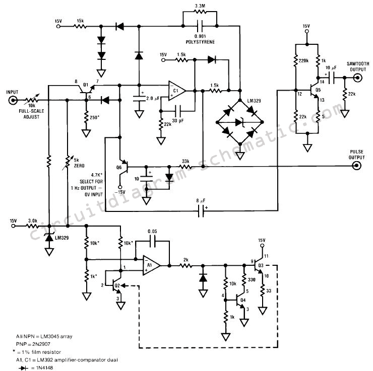
The circuit diagram depicts a design that achieves 0.25% exponential conformity over a frequency range of 20 Hz to 15 kHz using a single LM392 and an LM3045 transistor array. The exponential function is generated by Q1, whose collector...