
Video Camera switcher MAX454
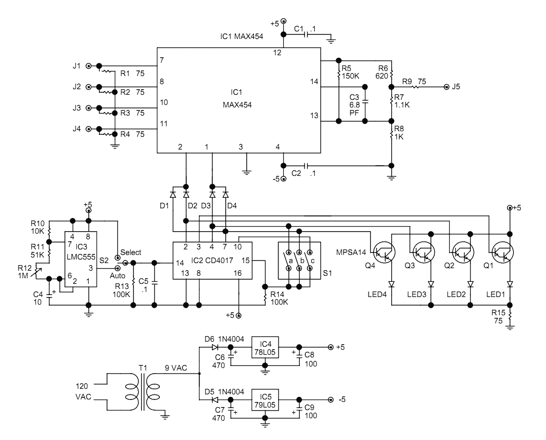
The video switcher circuit is designed to facilitate the seamless integration of multiple camera inputs into a single output display, making it particularly useful in applications such as live event broadcasting, security monitoring, and video production. The core functionality relies on the Maxim MAX454 integrated circuit, which serves as both a multiplexer and an amplifier, ensuring that the video output maintains high fidelity and low distortion.
The circuit's operation begins with the selection of the number of cameras to be used, which is determined by a DIP switch (S1) on the circuit board. This allows for flexible configurations ranging from two to four cameras. The system intelligently avoids displaying blank screens by only cycling through active camera inputs, thereby improving user experience.
In automatic mode, the switching rate can be adjusted via a panel-mounted potentiometer (R12), allowing users to set the interval between camera switches anywhere from one second to twenty seconds. This feature is complemented by a manual mode, where a momentary-toggle switch allows users to manually step through the camera inputs, providing control over which camera is displayed continuously.
The addressing of camera inputs is executed through a binary coding system facilitated by the CD4017 decade counter (IC2). This chip generates a unique output for each clock pulse received, which corresponds to the selected camera input. The outputs from IC2 are also linked to transistors (Q1-Q4) that drive indicator LEDs (LED1-LED4), providing visual feedback on which camera is currently active.
The clock pulses required for the CD4017 counter are generated by the LMC555 timer (IC3), which is configured to produce a variable frequency signal based on the resistance and capacitance values set by R10, R11, and C4. The toggle switch (S2) allows the user to select between automatic operation, manual selection, or an off state, ensuring versatility in operation.
Powering the circuit requires a 9-volt AC wall adapter, with additional components including rectifier diodes (D5, D6) and voltage regulators (IC4, IC5) ensuring stable voltage levels for the MAX454 and other ICs. The design emphasizes the importance of minimizing noise and crosstalk, which is achieved through careful PCB layout practices, including ground traces running parallel to signal traces.
In summary, this video switcher circuit is a robust solution for managing multiple video inputs, offering both automated and manual control options while ensuring high-quality output and minimal interference. Proper construction techniques, including the use of a printed circuit board, are critical to achieving optimal performance.The video switcher described here can display the output of two, three, or four cameras on a single monitor. The number of cameras is set by a DIP switch on the circuit board. That feature avoids blank displays if less than four cameras are used by sequencing through only the inputs that are connected to a camera.
In the automatic mode, the cameras are switched at a rate that can be varied with a panel mounted control. The switching rate can be set from about once per second to about once every 20 seconds. In the manual mode, one camera output is displayed continuously. A momentary-toggle switch is then used to step through the various cameras. The heart of the video switcher is a Maxim MAX454. That integrated circuit contains a four-way video multiplexer and an amplifier that operates as a low-impedance line driver. The resulting video output is high quality with very low phase distortion. The video inputs are selected by applying a binary number to the address inputs. The binary number is also used to light a series of LEDs that indicate whichh camera input is currently selected.
The circuit is powered by a 9-volt AC wall-adapter transformer, two diodes, and two voltage regulators. The binary addressing circuit is built around IC2, a CD4017 decade counter. That chip produces one positive output at a time on each of its ten outputs in sequence for every clock pulse.
The first four outputs at pins 3,2,4,and 7 are connected to transistors Q1- Q4. Those transistors drive LED1-LED4 through current limiting resistor R15. The outputs from IC2 (pins 2,4, and 7) are also decoded into binary logic by diodes D1-D4. The binary logic is sent to the address input lines of IC1. The number of cameras connected to the video switcher is set with S1. Each switch in S1 is connected to an output from IC2. If, for example, there are only two cameras connected to the video switcher, S1-a is closed. That connects the third output to IC2’s reset line. When IC2 advances to the third count, that output passes through S1-a to the reset, and IC2 resets to zero, activating the first camera. The sequence would be camera 1, camera 2, then back to camera 1. Closing S1-b or S1-c instead of S1-a will let the video switcher cycle through three or four cameras, respectively.
Clock pulses for the counter are generated by IC3, an LMC555 CMOS timer. The pulse rate and pulse width is controlled by C4, R10, R11 and potentiometer R12. By adjusting R12, the output frequency of IC3 can be controlled between 1 Hz and 1/20 Hz. The clock pulses from IC3 are connected to IC2 through S2, a three position toggle switch. Switching S2 to the auto position lets the pulses from IC3 select the next camera at a rate set by R12. When S2 is in its center-off position, no switching takes place, and whatever camera input is selected is passed through to the output.
The select position on S2 is a momentary contact. That position raises the clock input of IC2 to 5 volts, which increments the binary count and selects the next camera. When S2 is released, it springs back to its center-off position. The clock input of IC2 is then held at a low-logic level by R13. The MAX454 requires ±5 volts while the other ICs require only +5 volts. Power is supplied by AC adapter T1, rectifier diodes D5 and D6, regulators IC4 and IC5, and filter capacitors C6-C9.
Construction Because of the high frequency video signals involved, the video switcher should be built on a printed circuit board. The circuit is simple enough to fit onto a single-sided board with only two jumpers needed. A foil pattern is included for etching and drilling your own board. Alternatively, an etched board can be purchased from the source given in the parts list. A feature of that board design is ground traces that run between all of the video signal traces in order to keep induced noise and crosstalk between the signals to a minimum.
Weather you etch a board from the foil pattern or purchase one from the source in the parts list, use the parts-placement diagram in fig. 2 for component placement. It is easiest to install and solder the resistors and diodes first. Once those components are in place, scrap component leads can be used for the two jumper wires. Next, install S1 and sockets for IC2 and IC3. Do not use a socket for IC1, the MAX454 multiplexer. 🔗 External reference
Related Circuits
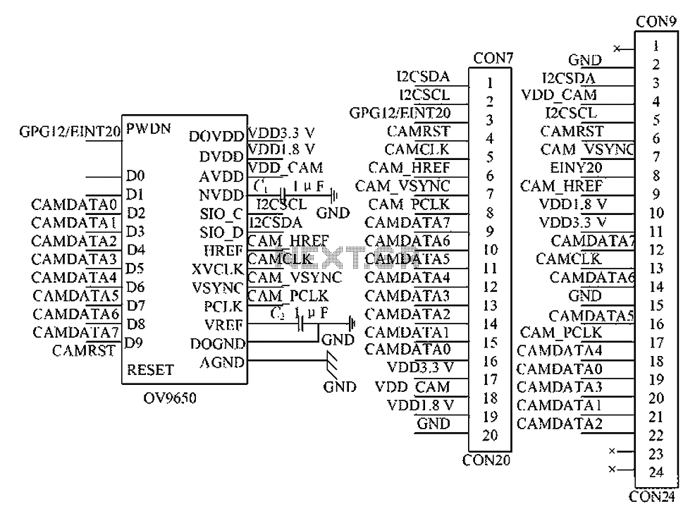
The circuit principle involves the OV9650 processor, which interfaces through three components: the SCCB interface, the data output interface, and the control interface. The SCCB interface is responsible for transferring initialization parameters from the processor's internal registers. It utilizes...
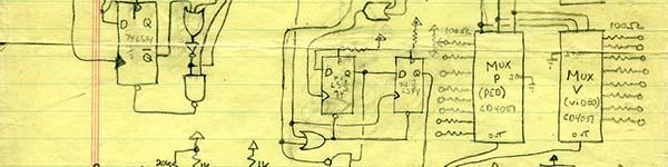
This example demonstrates the use of a pair of CD4051 multiplexers in parallel. The design incorporates elements from historical circuitry, particularly from Dave Jones' designs. This sequencer was constructed for a public access facility that primarily utilized a black...
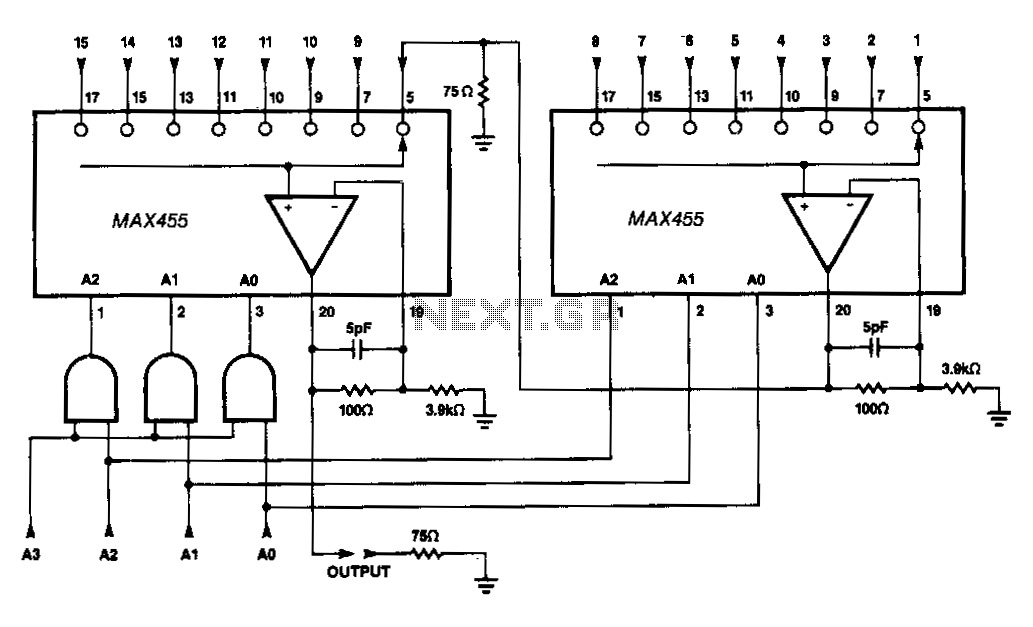
Two MAX455s can be cascaded to create a 1 of 15 video multiplexer (MUX) by connecting the output of one MUX to one of the input channels of a second MUX. Although the two devices are typically placed close...
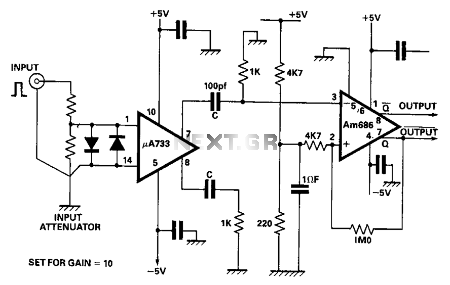
A video amplifier output arrives at a differentiation stage before the Schottky comparator. The typical propagation delay is reduced to 10 ns. The output pulse width is determined by the capacitance value, where C is 100 pF, resulting in...
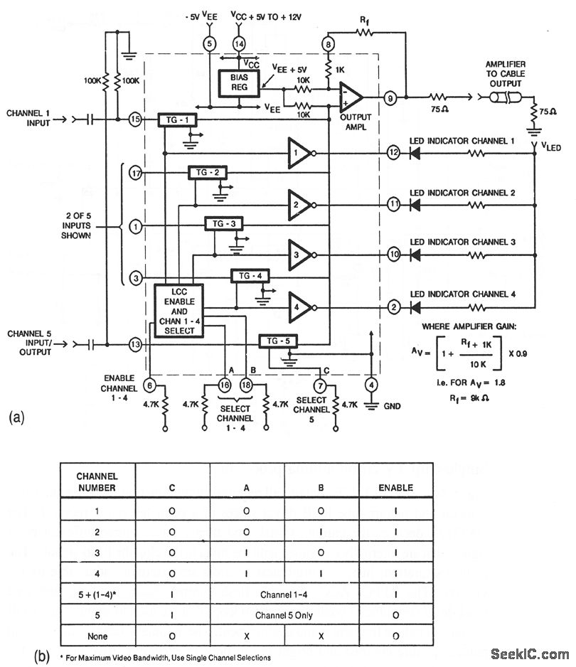
This circuit illustrates a CA3256 switch/amplifier configured for a direct-coupled output. One of four channels can be selected in parallel with channel 5. The analog switches of channels 1 to 4 are digitally controlled by logic. A VEE of...
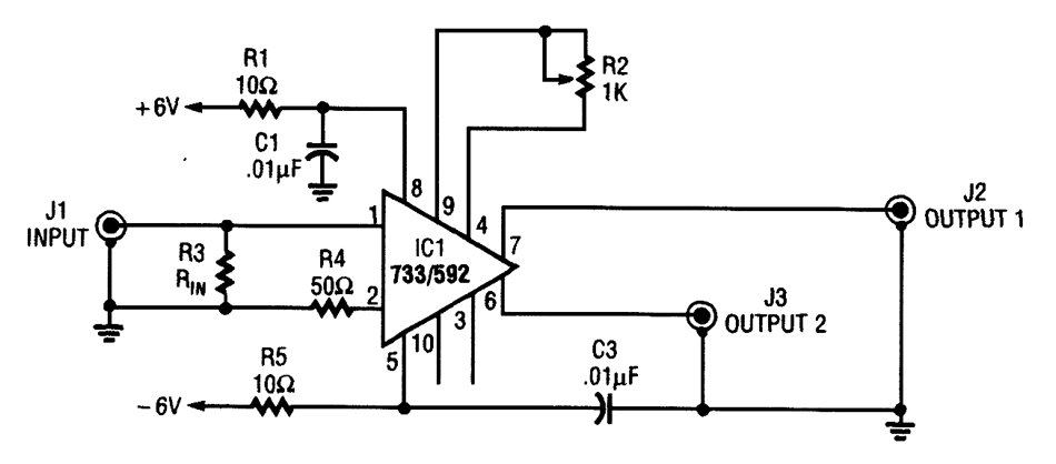
An NE592 or LM733 is utilized as a general-purpose video amplifier in this schematic. J2 and J3 deliver two anti-phase outputs. R2 serves as a gain control. The bandwidth is approximately 100 MHz. The NE592 and LM733 are integrated circuits...