
video signal amplifier using with lh0024
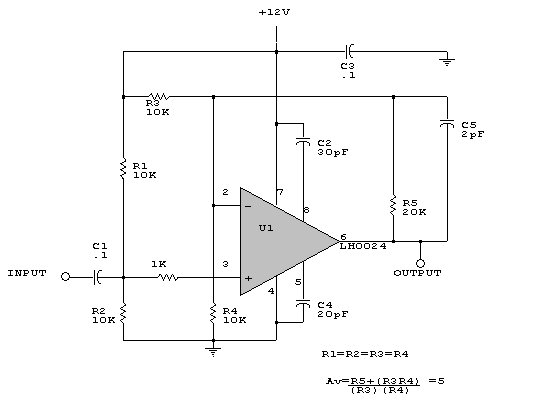
The LH0024 integrated circuit serves as a versatile component in various electronic applications, particularly in signal processing where amplification and switching are required. It is particularly well-suited for video signal amplification due to its ability to handle low voltage operations efficiently. The use of the 1N4148 diodes enhances the circuit's capability for fast switching, making it ideal for high-speed applications.
In the circuit design, the first stage with Q1 functions as an isolator, ensuring that the input signal does not load the source. This is critical in maintaining signal integrity, especially in video applications where high fidelity is essential. The second stage, utilizing Q2 in a common base configuration, is crucial for achieving the desired gain. The gain setting through TR2 allows for fine-tuning of the output to match the requirements of the connected load, ensuring optimal performance.
The frequency response of the circuit is carefully controlled using a combination of resistors and capacitors. R6 and C3 are selected to provide the necessary bandwidth while TR1 allows for additional adjustments, ensuring that the circuit can handle the frequency range of the video signals without distortion.
The final stage, represented by Q3, acts as a buffer to provide a stable output to the load, which is essential for maintaining signal quality when interfacing with other devices such as television receivers. The output impedance of 75 ohms is standard for video applications, ensuring compatibility with most video equipment.
Overall, the design is robust, with a power supply requirement of 12 V and a current draw of 50 mA, making it suitable for integration into various electronic devices where video signal processing is required.LH0024 IC small signal IC designed for general purpose switching and amplification due to its low voltage, low voltage and three different win the election 1N4148 silicon small signal diode planar epitaxial used for fast switching applications with a reverse voltage of 100 V and forward current of 150 mA In a video output signal is the high rate of frames selected for amplification of producing a finer. This is possible by placing the track between the video device and the reception lobby, where the video port of the television receiver is inserted. The construction is done simply by exploiting the operation of three transistors instead of IC and other supporting elements.
An isolator operating in the first phase of the Q1, which provides an interface for input impedance. Q2 manage the second phase, which leads to the common base configuration. In this phase, determine the earnings TR2 250 ohms cutting the lawn. To adjust TR2, it must be placed where an output voltage of 1 Vp-p is present, with a load of 75 ohms. The frequency response is regulated by a combination of R6, C3, and 500 ohms TR1. An output buffer is completed by Q3 of the third phase which provides an airline pilot with 75 ohms. The range of the circuit is stabilized with 12 V and 50 mA. 🔗 External reference
Related Circuits
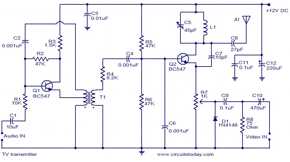
A simple two-transistor TV transmitter circuit that operates from 12V. It is compatible with PAL B and PAL G systems. The described circuit utilizes two transistors to create a basic television transmission system capable of operating on a 12V power...
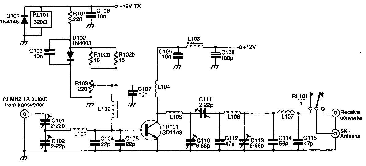
This 70 MHz RF power amplifier circuit utilizes the SD1143 transistor, which offers a gain of approximately 14 dB in this configuration. The design leverages the characteristics of a 175 MHz device. The RF power amplifier circuit designed around the...
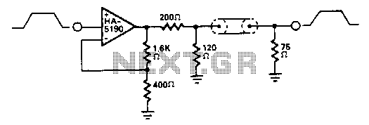
The HA-5190 can drive the 75-ohm coaxial cable with signals up to 2.5 V peak-to-peak without the need for current boosting. In this circuit, the overall gain is approximately unity due to the impedance matching network. The HA-5190 is a...
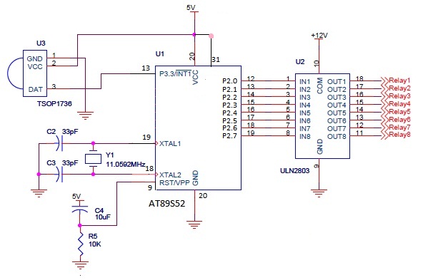
The infrared (IR) circuit is designed to control multiple devices using a TV remote. Unlike standard circuits that can typically switch only one device, this circuit allows for the operation of different devices with the same remote by utilizing...
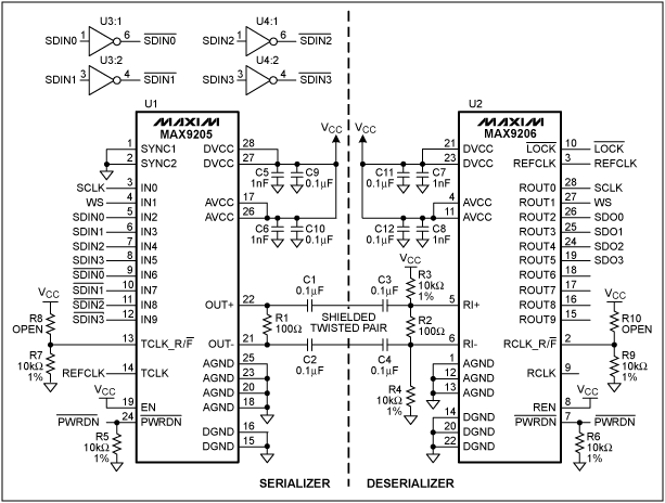
This application note outlines the transmission of I²S audio data streams between two audio components using a single shielded twisted-pair (STP) wire, employing the MAX9205 10-bit LVDS serializer and the MAX9206 10-bit LVDS deserializer. Low-voltage differential signaling (LVDS) serves...
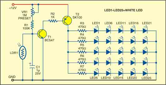
This sunlight-controlled lamp utilizes a light-dependent resistor (LDR) as the sunlight sensor and comprises a total of 25 high-brightness white LEDs. Each row of LEDs is connected in series with separate resistors. The operation of the circuit is straightforward....