
Voltage Controlled Frequency Divider with Variable Division Ratio
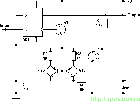
In the initial state, the direct output of D-flip-flop DD1 is "on," causing capacitor C1 to discharge through transistor VT4. Concurrently, transistor VT1 is turned off, disengaging the current mirror circuit. When a pulse is applied to the clock input of D-flip-flop DD1, the direct output switches to "off," and the inverted output turns "on." Subsequently, capacitor C1 begins to charge until the voltage at the D-input reaches a high value. The next clock pulse resets the trigger (DD1) for a duration of one period, and this process continues in a repetitive cycle.
The voltage-controlled frequency divider circuit operates by utilizing an adjustable delay circuit that enhances the flexibility of the frequency division process. The current mirror circuit effectively regulates the charging of capacitor C1, which is critical for determining the timing characteristics of the output pulses. The interaction between the D-flip-flop and the adjustable delay circuit allows for precise control over the output frequency based on the applied control voltage.
In practical applications, this circuit can be employed in various digital systems where frequency division is necessary, such as in clock generation, signal processing, and timing applications. The ability to adjust the delay provides additional versatility, enabling the circuit to adapt to different operational requirements. The synchronous nature of the output pulses ensures that the circuit maintains consistent timing relationships, which is essential for reliable performance in digital electronics.This voltage controlled frequency divider circuit (see figure in text) produces pulses of lower frequency that depends on the control voltage, and front edges of input and output pulses are synchronous. Actually, in this type of frequency dividers are used a monostable circuit, connected between an inverted output and D-input of D-flip-flop DD1, b
ut in this design the monostable circuit is replaced with an adjustable delay circuit. The adjustable delay circuit comprises a current mirror circuit, based on transistors VT2, VT3, and capacitor C1. A current through transistor VT3 is controlled by voltage Uctr < U/2, so a current of the same value goes to the second branch of the current mirror circuit.
This current charges the capacitor C1. Therefore, the rate of charging depends on the voltage Uctr. How this frequency divider circuit works. In the initial state, the direct output of D-flip-flop DD1 is "on", so the capacitor C1 is discharged by transistor VT4. In the same time, the transistor VT1 is turned off, so the current mirror circuit is disengaged. When a pulse is applied to the clock input of D-flip-flop DD1, the direct output changes its state to "off", and inverted output - to "on".
The capacitor C1 starts charging until a voltage at D-input reaches high value. The next clock pulse resets the trigger DD1 for the time of one period, and the process repeats over and over again. 🔗 External reference
Related Circuits
A voltage-controlled oscillator (VCO) is a type of oscillator in which the frequency of output oscillations can be adjusted by varying the amplitude of an input voltage signal. VCOs are commonly utilized in frequency modulation (FM), pulse modulation (PM),...
The iPod Shuffle has malfunctioned, likely due to a failure in the controller chip for the mini jack, resulting in the inability to detect the charger, PC connection, or headphones. The arc must be kept short to minimize distortions...
As the demand for VRM output current increases, the components and parts of the SR-Buck converter can no longer meet the requirements for the new generation microprocessors needing 100 A. Additionally, creating filtering inductance for high currents is quite...
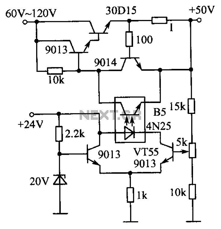
The circuit is illustrated. A standard driving transistor requires a higher breakdown voltage transistor (such as the FIG driving tube 9013). As the output voltage rises, the bias on VT55 increases, leading to an increase in the forward current...
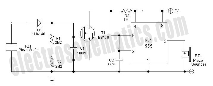
With the help of a simple ceramic piezoelectric detector, it is possible to assemble an interesting and useful impact sensor unit, which can be used to detect... An impact sensor unit utilizing a ceramic piezoelectric detector operates by converting mechanical...
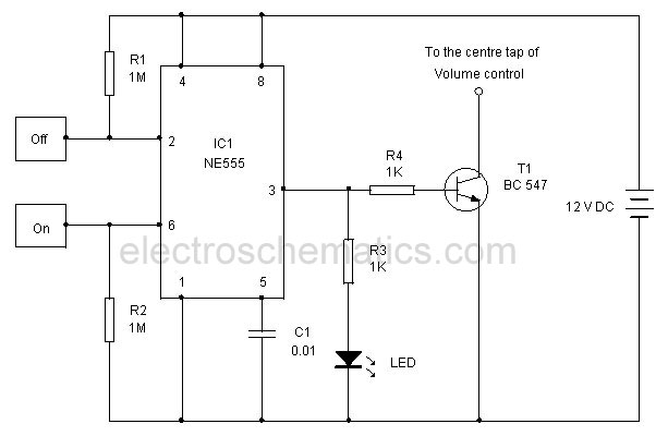
This touch-controlled musical bell circuit generates a musical tone whenever someone touches the designated touch point (TP). The circuit operates using two AA batteries and produces sufficient sound output. It utilizes the UM3481 integrated circuit, which is commonly employed...