
Voltage doubler circuit using NE555
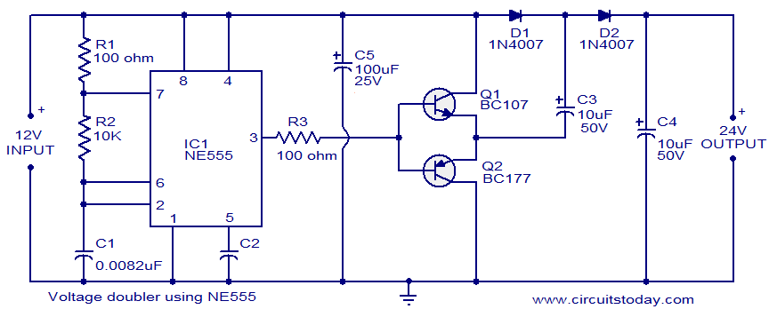
The voltage doubler circuit utilizing the NE555 timer is a straightforward design that leverages the timer's capabilities as an astable multivibrator to generate a square wave signal. This signal controls two transistors, which function as switches to alternately charge capacitors, thereby achieving voltage doubling. The NE555 timer is configured to oscillate at a frequency of approximately 9 kHz, which is suitable for this application.
Transistor Q1 and Q2 serve as the primary switching elements in the circuit. When Q2 is turned on, capacitor C3 charges to the input voltage, establishing a baseline voltage level. Upon switching, when the output from the NE555 goes high, Q1 turns on, allowing capacitor C4 to charge to a higher voltage, which is effectively the sum of the input voltage and the voltage across C3. This results in a doubled output voltage, making the circuit beneficial for applications requiring a higher voltage from a lower voltage source.
The design includes capacitors C3 and C4, which are essential for storing and transferring charge. C3 acts as an initial charge storage element, while C4 serves as the output capacitor that provides the doubled voltage. The circuit's limitation of 50 mA output current is a critical consideration, as exceeding this threshold can lead to a drop in output voltage due to the transistors' inability to handle higher currents effectively.
In practical applications, this voltage doubler circuit is advantageous for powering low-current devices, where the simplicity and compactness of the design can be beneficial. However, users should be aware of the potential instability in the output voltage and the current limitations when designing systems that incorporate this circuit.The circuit diagram of a very simple voltage doubler using NE555 timer is shown here. Here IC NE555 is wired as an astable mutivibrator operating at around 9KHz. The base of the two transistors (Q1 and Q2) is shorted and output of the astable multivibrator (pin 3) is connected to it. When the output of astable multivibrator is low, Q1 will be OFF and Q2 will be ON. The negative terminal of the capacitor C3 will be shorted to ground through T2 and it will be charged to the input supply voltage. When the output of the astable multi vibrator is high, transistor Q1 will be ON and transistor Q2 will be OFF.
The capacitor C4 will be charged to the voltage across capacitor C3 plus the input supply voltage (that is double the input voltage). This is how the circuit works. This voltage doubler circuit can deliver only up to 50mA output current and above that current limit the output voltage will be dramatically reduced.
The actual output voltage will be around 19V for a 12V DC input and also the output voltage will be a bit unstable. Anyway, for low current applications this circuit is well enough. CircuitsToday has introduced an online store where you can buy books that give you a better understanding on the applications of 555 IC.
These books have been reviewed in detail and the links to buy them is also provided. Check it out:- 3 Great Books to Learn 555 Timer Circuits and Projects. 🔗 External reference
Related Circuits
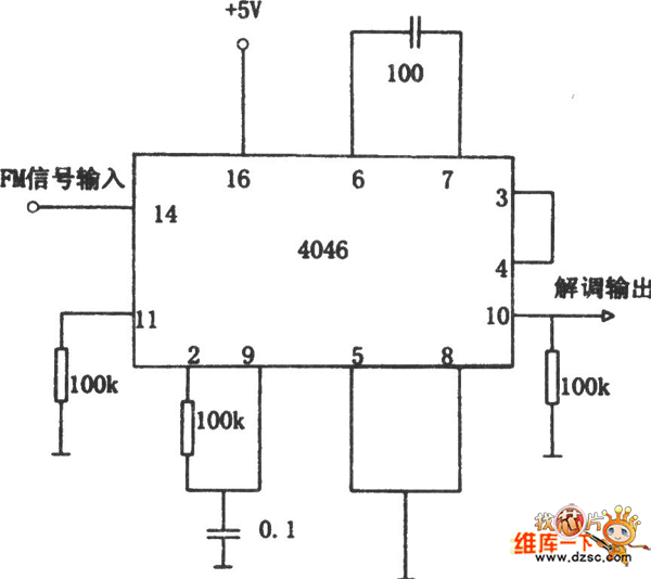
The FM demodulator circuit, as illustrated in the figure, utilizes a 4046 Phase-Locked Loop (PLL) integrated circuit to convert the intermediate frequency FM input signal into a lower frequency output. The FM demodulator circuit based on the 4046 PLL IC...

A gas leak detector circuit that detects the leakage of LPG gas and alerts the user through audio-visual indications. The circuit operates off a 9V PP3 battery. A Zener diode is used to convert 9V into 5V DC to...
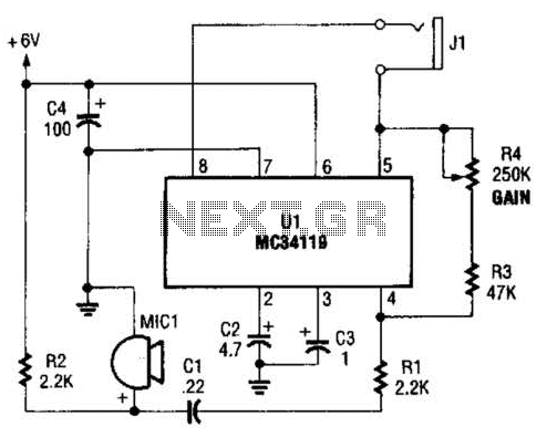
The first amplifier circuit is a bird phone. In this circuit, the electret microphone (MIC1) is mounted in the neck of a large plastic funnel. The amplifier, built around an MC34119, is then placed outside of the funnel with...
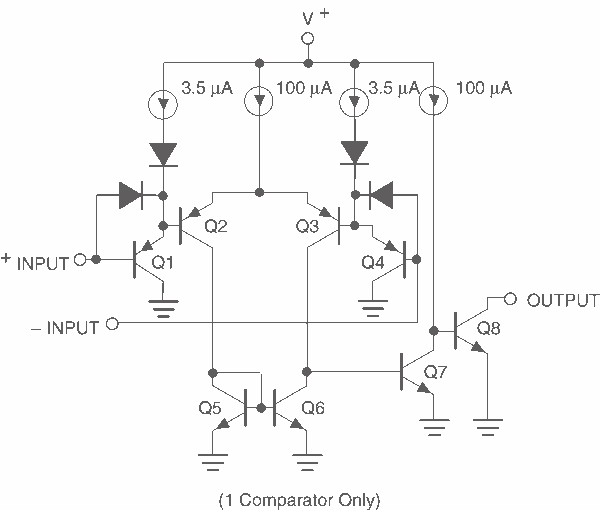
This page provides basic information about voltage comparator integrated circuits and is to act as reference material for other circuits. The circuits shown are based on the LM339 Quad Voltage Comparator chip or the LM393 Dual Voltage Comparator chip....
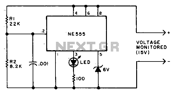
Due to the low duty cycle of the flashing LED, the average current drain is 1 mA or less. The NE555 will trigger the LED when the monitored voltage falls to 12 volts. The ratio of R1 to R2...
This design features a signal logic tester that utilizes a common cathode seven-segment display. The display indicates a logic level "1" (represented by an "H" on the display) or a logic level "0" (represented by an "L" on the...