
Voltage Doublers
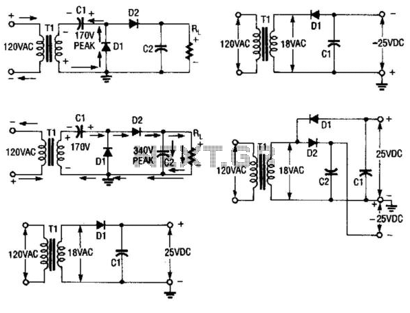
The described circuit operates as a voltage doubler utilizing two half-wave rectifiers. In the first half-cycle, when D1 is forward-biased, it allows current to flow, charging C1 to 170 V. This voltage is established due to the peak input voltage and the characteristics of the diodes. D2 remains off during this phase, preventing any current flow through its path. C2 discharges its stored energy through the load resistor RL, providing power to the load.
Upon entering the second half-cycle, the polarity of the input voltage reverses. This reversal places C1 in series with the input voltage, effectively doubling the voltage across the load. The total voltage seen by the load becomes 340 V at peak due to the additive nature of the series connection. In this phase, D1 becomes reverse-biased and ceases to conduct, while D2 turns on, allowing current to flow through it. The current now divides between C2 and the load resistor RL, with C2 continuing to supply energy to the load.
This arrangement of two half-wave rectifiers, one configured for positive output and the other for negative output, results in a full-wave voltage doubler. The output voltage is effectively doubled compared to the input voltage, making this circuit useful in applications where higher voltage levels are required from a lower voltage AC source. The continuous cycling of the diodes ensures that energy is efficiently transferred and stored, maximizing the output voltage available for the load. The design is particularly advantageous in power supply applications where compact size and high efficiency are desired. During the first half-cycle (Fig. 99-5(a)), Dl conducts, D2 cuts off, CI changes to 170 V peak, and C2 discharges through RL. For the second half-cycle (Fig. 99-5(b)), the input polarity is reversed, and both the input and CI are in series, which produces 340 V (peak). Now, Dl cuts off, while D2 conducts, and the current divides between C2 and Rl, the cycle then repeats.
Two Half-Wave Rectifiers, one with a positive output (Fig. 99-5(c)) and one negative (Fig. 99-5(d)), combine to make a full-wave voltage doubler (Fig. 99-5 (e)). 🔗 External reference
Related Circuits
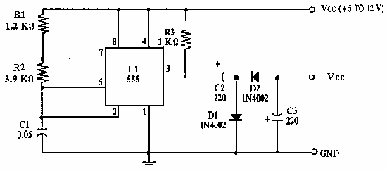
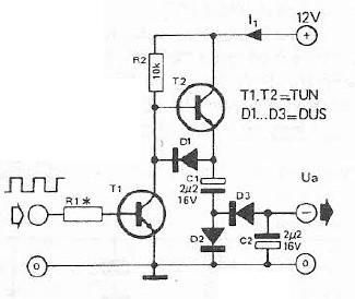
This circuit inverts the polarity of the input. Output is limited to less than 200mA. More: U1 NE555 timer IC R1 1.2k ohm resistor R2 3.9k ohm resistor R3 1k ohm resistor C1 0.05 uF ceramic capacitor C2, C3...
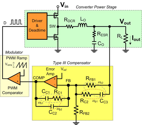
Before designing with one of today's powerful buck regulator ICs, it is essential to have a thorough understanding of voltage mode control and compensation. Voltage mode control is a widely used method in switching power supplies, particularly in buck converters....
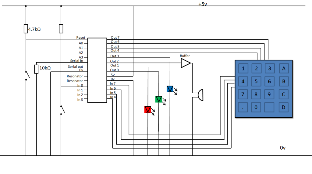
A keypad lock is being developed using a PIC microcontroller and a passive keypad with 8 pins, consisting of 4 input and 4 output pins. Each input pin corresponds to a row of numbers on a 4x4 keypad, while...
Voltage inverter circuit design electronic project using few electronic components The voltage inverter circuit is a fundamental electronic project that converts direct current (DC) to alternating current (AC). This circuit is particularly useful in applications where AC voltage is required...
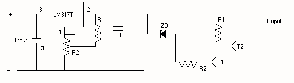
It is a voltage regulator that allows a 6v portable supply to be derived from the 12v car battery. You can add a 6.2V zener diode and a LED to warn you when the input supply is overvoltage. If...
Two examples of the most common types of Voltage followers (buffers). You can find some theory behind them in our amplifier gain and buffer amplifier pages. This first circuit is a very simple one transistor voltage follower. Consists of...