
Voltage Level Detector Circuit
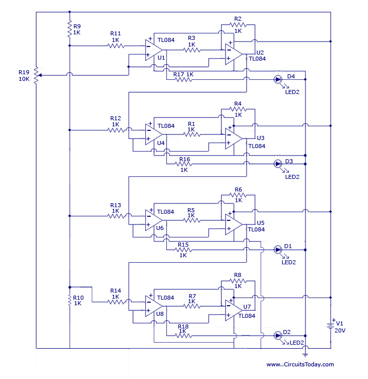
The circuit design integrates a multi-stage architecture to facilitate efficient analog-to-digital conversion. Each stage's operational amplifiers are configured to ensure that the signal is accurately amplified and compared against a predetermined reference voltage. The use of TL084 OP-AMPs is notable due to their low noise characteristics and high-speed performance, making them suitable for applications requiring rapid signal processing.
The configuration allows for dynamic adjustment of the number of stages, enabling scalability based on the desired resolution and speed of the ADC. The non-inverting amplifier stage ensures that the signal is amplified without phase inversion, which is critical for maintaining signal integrity throughout the conversion process.
The reference voltage is created using a voltage divider network formed by two resistors, which provides a stable reference point for the comparator. This setup is essential for ensuring accurate comparisons, as any fluctuation in the reference voltage can lead to erroneous digital output.
The binary output is represented by four LEDs, which provide a visual indication of the digital count derived from the analog input. This feature enhances the circuit's usability by allowing real-time monitoring of the conversion process.
Overall, the design represents a thoughtful synthesis of speed and component efficiency, addressing the inherent trade-offs between Flash and Successive Approximation ADCs, while also acknowledging the practical limitations of achieving exact gains in real-world applications.The design came from the interest of finding a new technique of analog to digital conversion. The two types of ADC (Analog to Digital Converter) that inspired me in the development of this circuit are Flash Type ADC and Successive Approximation Type ADC. The Flash Type ADC is the fastest ADC available in the market (highest sampling rate 120 Msps) but it uses a huge number of OP-AMPS. On the other hand Successive Approximation Type ADC uses fewer components but its speed is dependent upon the clock frequency provided to it. I was looking for a technique that can give a trade-off between this two, the result of which is this circuit.
The working of this circuit is similar to that of decimal fraction to binary fraction conversion. For this purpose, the circuit amplifies a signal and compares it to a reference voltage. The circuit can be divided into a number of stages. Number of stages can be increased or decreased according to need. Each stage contains two OP-AMPs(TL084). One of them (OP-AMP at the left side) is used for comparison purpose. The other (OP-AMP at the right side) is used as a non-inverting amplifier with a fixed gain (EXACTLY 2). The input voltage is connected to the non-inverting pin/terminal of each OP-AMP. The digital output is obtained from the output of the comparing OP-AMP and the output of the amplifier OP-AMP is fed to the input of the next stage.
To obtain a reference voltage, two resistors are used. An input voltage is applied. The OP-AMP used as a comparator compares the input voltage with the reference level. If it exceeds a certain reference level, the comparator output goes high and there is amplification along with subtraction operation is performed by the amplifying OP-AMP. If the input voltage is less than the reference voltage, only the amplification operation is performed.
The output of the amplifier OP-AMP is inherited to lower stages. To see if the circuit is working or not, use a potentiometer, connect its two ends to the two poles of the battery, connect the wiper to the first stage of the circuit. Now as the potentiometer is swiped across its range, a count can be observed represented by the four LED`s.
It will be a binary count, either upward or downward. The gain of the amplifier must be 2. Small error in higher stages will deteriorate the performance of lower stages and is un-avoidable since practically a gain, exactly 2 is un-obtainable. Even the 4 stage circuit will show up level loss. 🔗 External reference
Related Circuits
The ICM7226 is a fully integrated Universal Counter and LED Display driver. It combines a high-frequency oscillator, a decade timebase counter, an 8-decade data counter and latches, a 7-segment decoder, digit multiplexer, and segment and digit drivers, which can...
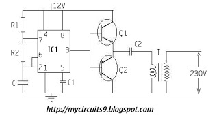
The timer IC (NE555) is configured as an astable multivibrator in this circuit. It generates an alternating non-sinusoidal output waveform as soon as a supply voltage of 12V is applied. Therefore, alternating voltage is produced from direct current (battery)....
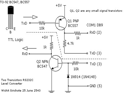
To connect a microcontroller project to the COM port of a PC, an RS-232 converter is required. Various chips are available to address this need, such as the MAX232 and DS275. The RS-232 standard is widely used for serial communication...
More: A comprehensive electronic schematic description is required to provide an overview of the circuit's functionality, components, and operation. The schematic should include a clear representation of the electronic components involved, such as resistors, capacitors, diodes, transistors, integrated circuits,...
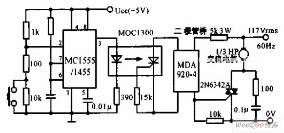
The switch shut-off time delay circuit consists of a timer, optocouplers, a bridge SCR, and an SCR AC switch. When the control button is released, it allows the motor or other AC power to remain active for one hour....
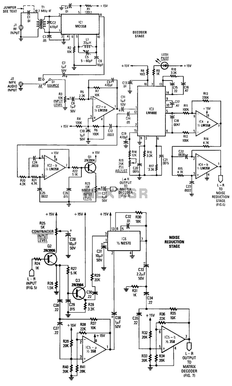
A block diagram of the stereo-TV decoder illustrates the overall relationships between the distinct sections of the circuit, while additional details of each subsection are provided. The decoder section is centered around TCI, a standard 4.5-MHz audio demodulator. The...
Warning: include(partials/cookie-banner.php): Failed to open stream: Permission denied in /var/www/html/nextgr/view-circuit.php on line 713
Warning: include(): Failed opening 'partials/cookie-banner.php' for inclusion (include_path='.:/usr/share/php') in /var/www/html/nextgr/view-circuit.php on line 713