
Stereo Tv Decoder Circuit
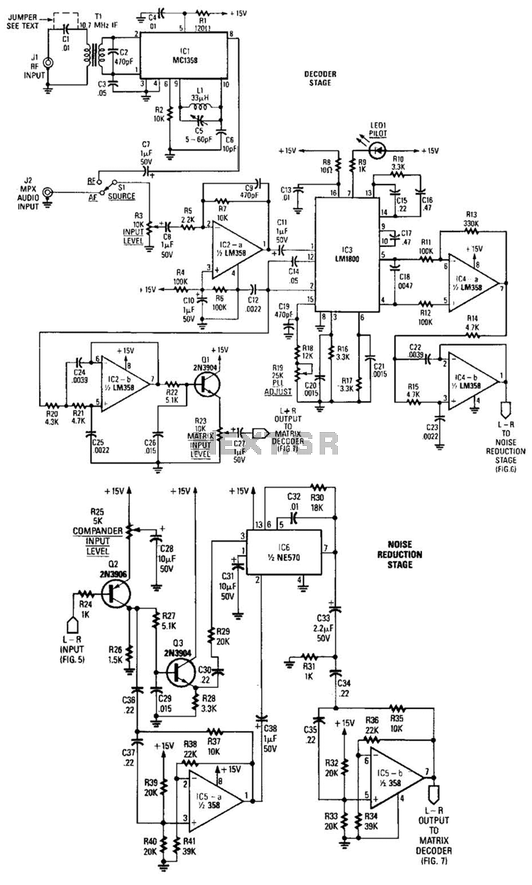
Capacitor C18 bridges the left and right channel outputs of the demodulator. While it slightly diminishes high-frequency separation, it also mitigates high-frequency distortion. The L + R signal is extracted from the LM1800 at pin 2, appearing at the output of an internal buffer amplifier. The raw L - R signal is sent to IC4-b, which functions as a 12-kHz low-pass filter. The L + R signal also passes through a 12-kHz low-pass filter to ensure equal phase shift for both signals. The L - R signal is then processed by Q2, which introduces a level control to the L-R signal path, providing low source impedance for subsequent circuits and inverting the signal by 180 degrees. This inversion compensates for the 180-degree inversion in the compander.
The expander stage follows, with a 75-µs de-emphasis network (R27 and C29) located at the collector of Q2, functioning similarly to the network associated with Q1. Q2 drives both Q3 and IC5-a, a -12 dB per octave high-pass filter. The output of this filter feeds the rectifier input of IC6, an NE570. The 75-Hz high-pass filter at the rectifier input prevents low-frequency noise, such as hum and 60-Hz sync buzz, from causing pumping or breathing in the L-R signal. The NE570 contains an onboard op amp, with its inverting input accessible directly at pin 5 and via a 20-kΩ series resistor at pin 6. The 18-kΩ resistor (R30) combines with the internal resistor and C32 (0.01 µF) to create a first-order filter with a 390-µs time constant. As the internal op amp operates in the inverting mode, the - (L-R) signal is restored to the correct (L-R) form.
The output from the expander drives another 75-Hz high-pass filter, this one a third-order type providing -18 dB per octave roll-off, which helps prevent low-frequency noise from appearing at the decoder's output. At this stage, the (L - R) signal is largely restored to its condition prior to dBx companding at the transmitter. The L + R signal from IC3 is routed to a 12-kHz low-pass filter, 102-b, with a -12 dB per octave slope. The output of this high-pass filter is applied to a 75-µs de-emphasis network (R22 and C26), effectively restoring the L + R audio signal. Q1 is configured as an emitter follower to provide a high load impedance for the de-emphasis network and a low source impedance for level control R23. The L + R signal is then sent to the matrix decoder.
Op amps IC7-a and IC7-b are employed to recover the individual channels. IC7-b is set up as a unity-gain difference amplifier, with the (L + R) signal applied to its inverting input and the (L - R) signal to the non-inverting input. Consequently, the output of IC7-b can be expressed as -(L + R) + (L - R) = -L + L - R - R = -2R. Similarly, IC7-a is configured as a mixing inverting amplifier, where both sum and difference signals are applied to the inverting input. Thus, the output of IC7-a is (L + R) - (L - R) = -L - R - L + R = -2L. The inversion of both channels preserves the stereo relationship. The two op amps in IC8 provide an additional amplification stage to drive a pair of stereo headphones. If headphone use is not intended, or if the stereo's headphone jack suffices, all components to the right of line-output jacks J3 and J4 can be omitted.
The noise reduction stage compands the L-R signal and emulates dbx-style processing. True dbx processing, however, is not feasible in a home-built circuit due to the unavailability of dbx ICs. The matrix stage separates the L + R and L - R signals into their respective left and right channel components. Op-amp IC8 and its associated components provide an optional headphone output. If headphone use is not desired, or if the amplifier's headphone jack will be utilized instead, all components to the right of jacks J3 and J4 can be deleted. A block diagram of the stereo-TV decoder is shown in A. It shows the overall relationships between the separate sections of the circuit; through show the details of each subsection. The decoder section centers around TCI, a standard 4.5-MHz audio demodulator. The output of IC1 is routed to SI, which allows you to choose between the internally demodulated signal and an externally demodulated one.
Buffer amplifier IC2- a then provides a low-impedance source to drive IC3, an LM1800 stereo demodulator. When IC3 is locked on a stereo signal, the outputs presented at pins 4 and 5 are discrete left- and right-channel signals, respectively.
In order to provide noise reduction to the L-R signal, you must recombine the discrete outputs into sum and difference signals. Op amp IC4-a is used to regenerate the L-R signal. It is wired as a difference amplifier, wherein the inputs are summed together (+L -R~). Capacitor C18 bridges the left- and right-channel outputs of the demodulator. Although it decreases high-frequency separation slightly, it also reduces high-frequency distortion. The L + R signal is taken from the LM1800 at pin 2, where it appears at the output of an internal buffer amplifier. The rawL -R signal is applied to IC4-b, a 12-kHz lowpass filter. The L + R signal is also fed through a 12-kHz low pass filter in order to keep the phase sliift undergone by both signals equal.
Next, the L -R signal is fed to Q2. It allows you to add a level control to the L-R signal.path; it provides a low source impedance for driving the following circuits, and it inverts the signal 180. Inversion is necessary to compensate for the 180 inversion in the compander. Next comes the expander stage. At the collector of Q2 is a 75-8 de-emphasis network (R27 and C29) that functions just like the network that is associated with Ql.
Note that Q2 feeds both Q3 and IC5-a, a -12-dB per octave high-pass filter. The output, of that filter drives the rectifier input of IC6, an NE570. The 75-Hz high-pass filter at the rectifier input helps to prevent hum, 60-Hz sych buzz, and other low- frequency noise in the L-R signal from causing pumping or breathing. The NE570 contains an on-board op amp; its inverting input is available directly at pin 5 and via a 20-kQ series resistor at pin 6.
The 18-kQ resistor (R30) combines with the internal resistor and C32 (0.01 ) to form a first-order filter with a 390- time constant. Because the internal op amp operates in the inverting mode, the -{L-R) signal is restored to the proper (L-R) form.
The output of the expander drives another 75-Hz high-pass filter, but this one is a third-order type that provides -18 dB per octave rolloff. It is used to keep low-frequency noise from showing up at the output of the decoder. At this point, the (L - R) signal has been restored, more or less, to the condition it was in before it was dBx companded at, the transmitter.
The L+R signal from IC3 is fed to a 12-kHz low-pass filter, 102-b, with a -12 dB per octave slope. The output of the high-pass filter is applied to a 75 de-emphasis network (R22 and C26). The L + R audio -signal is now restored properly. Ql is wired as an emitter follower to provide a high load impedance for the de-emphasis network and a low source impedance for level control R23. Next, the L + R signal is fed to the matrix decoder. Op amps IC7-a and IC7-b are used to recover the individual channels. First, IC7-b is configured as unity-gain difference amplifier. The (L + R) signal is applied to its inverting input, and the (L-R) signal is applied to the noninverting input.
Therefore, the output of IC7-b can be expressed as ~(L + R) + (L-R) =-L+L-R-R = -2R. Similarly, .10 7-a is configured as a mixing inverting amplifier. Here, however, both sum and difference signals are applied to the inverting input. So, the output of IC7-a is {L + K) - (L - R) = -L - R - L + R = -2L. Because both channels have been inverted, the stereo relationship is preserved. The two op amps in 108 provide an additional stage of amplification to drive a pair of stereo headphones. If you don`t plan to use your headphones, or if you are content to use only your stereo`s headphone jack, all components to the right of line-output jacks J3 and J4 can be deleted.
THE NOlSE*REDUCTION STAGE compands the L-R signal, and emulates dbx-style processing. As described elsewhere in this article (see box), true dbx processing is not currently possible in a home-built circuit due to the inavailability of the dbx IC`s. THE MATRIX STAGE separates 1 he L + R and L-R signals into the left- and right-channel components. Op-amp`lC8 and associated components provide an optional headphone output. If you do not wish to drive a pair of headphones, or plan to use your amplifier s headphone jack for that purpose, all components to the right of jacks J3 and J4 can be deleted.
🔗 External reference
Related Circuits
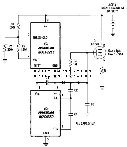
Deep discharge can damage a rechargeable battery. By disconnecting the battery from its load, this circuit halts battery discharge at a predetermined level of declining terminal voltage. Transistor Q1 acts as the switch. The overall circuit draws about 500µA...
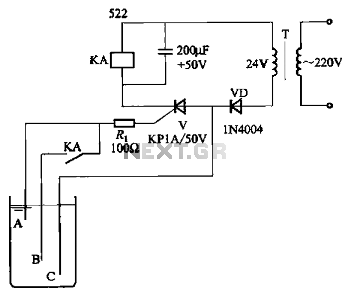
The circuit depicted in Figure 11-14 utilizes a unidirectional thyristor within liquid level automatic control systems. It incorporates electrodes that serve as sensing elements for detecting the level of water or other conductive liquids. The circuit features a current...
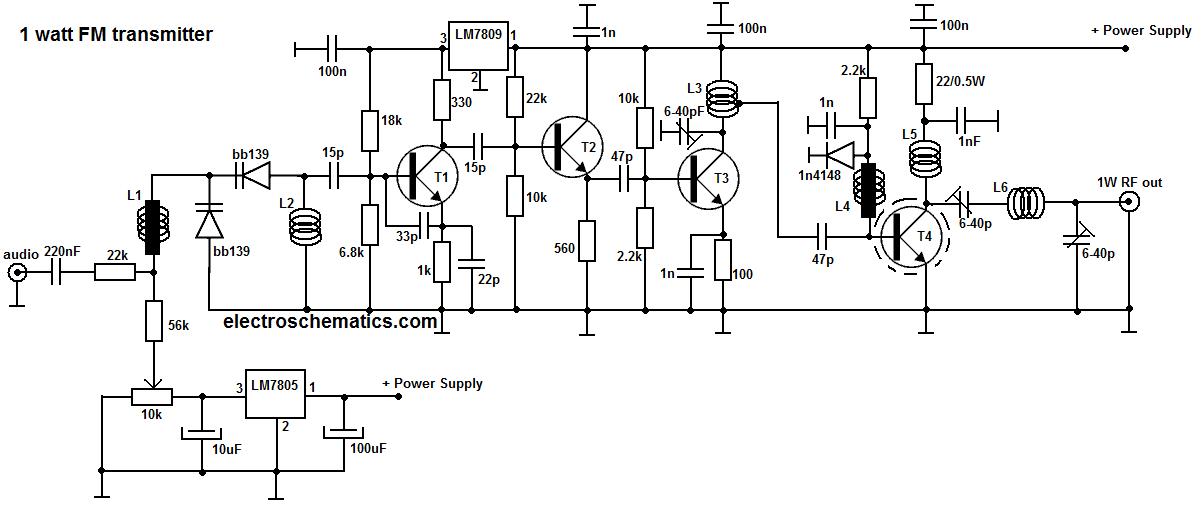
This portable FM transmitter features a limiter, a microphone amplifier, and PLL digital tuning, all integrated onto a single circuit board. The RF power output can be switched between 1 W (high) and 0.2 W (low). The schematic is...
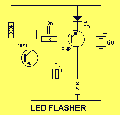
This is a very simple project using a printed circuit board and 8 components. It will flash an ordinary 3mm or 5mm (1/8" or 1/4") LED at a rate of about one flash per second. This circuit works on...
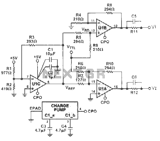
The circuit can incorporate a buffer gate at the input to ensure compatibility with TTL or other logic levels. This design is intended for a TTL 0V circuit to accommodate a 3.5V input signal swing. Additionally, it generates a...
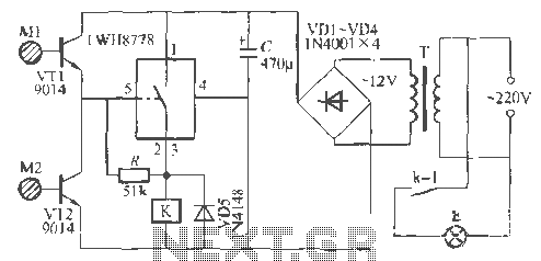
The Rw A77S power system utilizes an integrated circuit fabrication design featuring a dual touch light switch. It employs a transformer (T) for power conversion, a rectifier (VD4), and a capacitor (C) for filtering, resulting in a 12V DC...