
VOLTAGE TO CURRENT CONVERTER

The voltage-to-current converter circuit employs three operational amplifiers (op-amps) configured to provide precise control over the output current. The primary function of this circuit is to convert an input voltage (Vin) into a proportional output current (IOUT) based on the resistance value of R6. The relationship between the input voltage and output current is defined by the equation IOUT = Vin/R6, where R6 serves as a critical component in setting the current output.
In this configuration, the first op-amp is typically used for voltage amplification, ensuring that the input signal is adequately processed. The second op-amp may be configured as a differential amplifier to enhance the accuracy of the output current, while the third op-amp is employed as a buffer to drive the power transistors (T1 and T2) effectively. This arrangement allows for improved linearity and stability of the output current across varying load conditions.
The output resistance of the circuit is exceptionally high, exceeding 50 MΩ, which is advantageous for applications requiring minimal loading on the input source. The ability to adjust the output current from a minimum of 1 mA to the maximum ratings of the power transistors (T1 and T2) makes this converter suitable for a wide range of applications, including signal processing and driving high-impedance loads.
In summary, this voltage-to-current converter design offers a robust solution for converting voltage signals into precise current outputs, leveraging the capabilities of multiple operational amplifiers and power transistors to achieve high performance and adaptability in various electronic applications.This voltage to current converter uses three op amps to drive a pair of power transistors. The current output is calculated as: IOUT=Vin/R6 Output resistance is over 50 M?. IOUT can range from 1 mA to the current ratings of T1 and T2.. 🔗 External reference
Related Circuits
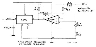
The datasheet contains application circuit diagrams for the L200, including a Programmable Voltage Regulator, a High Current Voltage Regulator with Short Circuit Protection, a Digitally Selected Regulator with Inhibit, a Programmable Voltage and Current Regulator, a High Current Regulator...
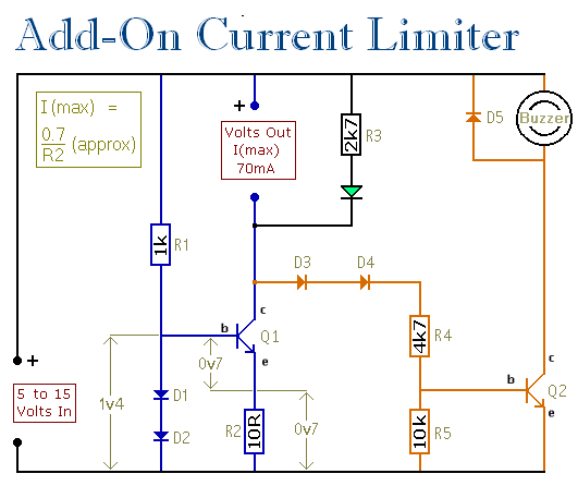
This circuit establishes a maximum limit on the current available from the output terminals by controlling the maximum current that can flow through Q1. The output terminals are in series with Q1, meaning that limiting the current through Q1...
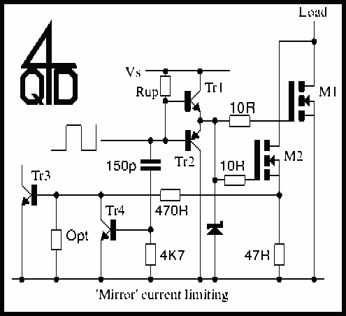
The circuit shows the method of mirror current sensing a MOSFET. A fully conducting MOSFET is resistive and behaves exactly as a resistor. It therefore you limit the voltage across the MOSFET when it is conducting you automatically limit...
Suppose there is a need to utilize a 5V DC power supply capable of delivering up to 100mA, but only a single AA 1.5V battery is available. To achieve this, a DC to DC converter must be employed. To convert...
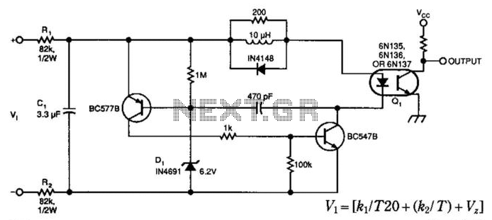
A simple voltage-controlled oscillator (VCO), coupled to instrumentation by an optoisolator, allows for the measurement of high voltages. The component values are suitable for a 0 to 600 V input range, with power dissipation in resistors RI and R2...
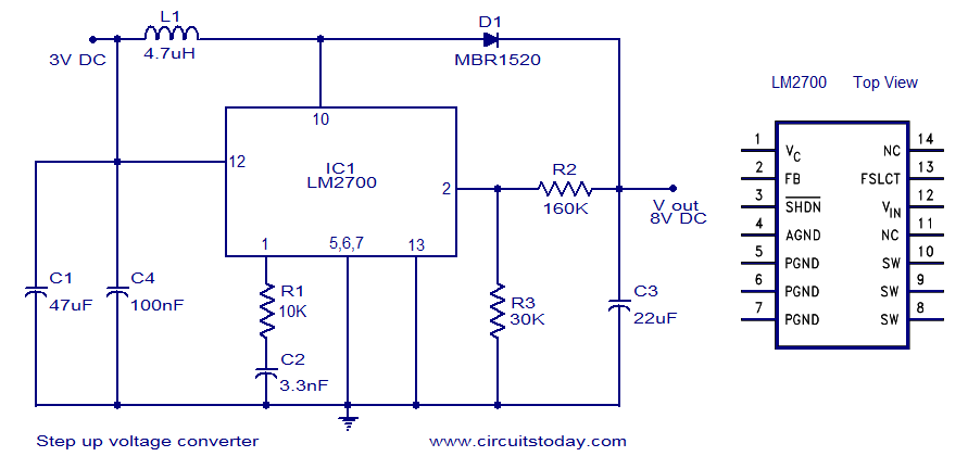
A simple DC to DC step-up voltage converter circuit schematic using the LM2700, which is a step-up switching converter. The LM2700 is a versatile step-up switching converter designed to efficiently convert a lower input voltage to a higher output voltage....