
Current Limiter - Support Material
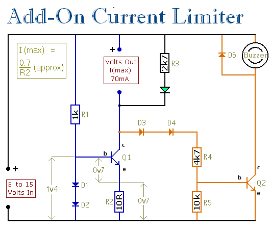
That is - you set a limit on the amount of current available from the output terminals. = The key to limiting the Q1 emitter current - is to set a maximum limit on the transistor`s base voltage. That`s the purpose of D1 & D2 Each diode has a forward voltage drop of about 0v7. The two together prevent the base voltage of Q1 from rising above about 1v4. It may be lower than 1v4 - but it cannot go higher than 1v4. In effect - D1 & D2 are acting like a 1v4 zener diode. = The voltage on the base of a silicon NPN transistor is always about 0v7 higher than the voltage on its emitter.
So - when D1 & D2 prevent the voltage on the base of Q1 from rising above 1v4 - they also prevent the voltage across R2 from rising above about 0v7. It may be lower than 0v7 - but it cannot go higher than 0v7. = If the maximum possible voltage across R2 is 0v7 - then the maximum possible current through it is 0.
7 G· R2. In the drawing - R2 is a 10 ohm resistor. And the maximum current that will flow through it is: - 0. 7 G· 10 = 70mA. = R2 is connected in series with Q1 and the output terminals. If 70mA is the largest current that can flow through R2 - it`s also the largest current that will flow through the transistor. And - it`s the maximum current that will flow between the output terminals - even if they`re shorted together.
= To understand how this works - first consider what would happen if the diodes were not present - and the output terminals were shorted together. = As the base current through R1 begins to turn the transistor on - current will start to flow through both the transistor and R2.
So the voltage across R2 will begin to rise. This causes the voltage on the emitter to rise. And - since the base is always 0v7 higher than the emitter - the voltage on the base is carried upwards by the emitter. = Eventually, virtually the whole of the supply voltage will appears across R2. So - with a 12-volt supply - the maximum current flowing through the output terminals, the transistor and R2 is roughly (V G· R) = (12 G· 10) = 1.
2 amps = Now consider the same situation with D1 & D2 in place. The two diodes prevent the base of Q1 from rising above 1v4. This means that the base voltage cannot ride up on the back of the emitter. = The base cannot go higher than 1v4. So the emitter voltage cannot go higher than 0v7. And the highest current that will flow between the output terminals - is one that cause a drop of 0v7 across R2. That is: I(max) = (V G· R2) = (0. 7 G· 10) = 70mA. = Consider what would happen if the voltage on the emitter tended to rise above 0v7. The base-emitter junction would no longer be forward biased. So the transistor would begin to turn off. This would lead to a fall in the current flowing through R2 - resulting in a drop in the voltage across it.
This drop in voltage would restore the forward bias to the base-emitter junction - and the current through R2 wou 🔗 External reference
Related Circuits
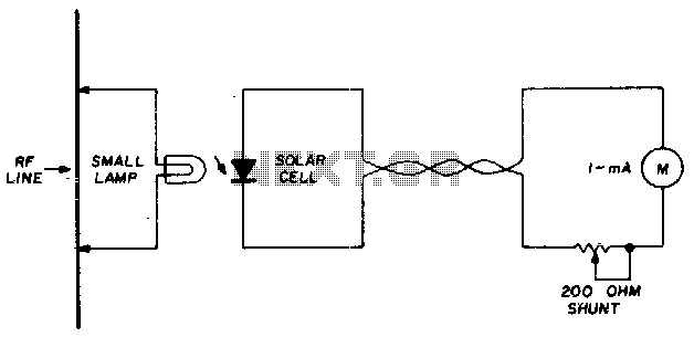
A suitable pilot lamp is illuminated by a small sample of RF energy and energizes an inexpensive solar cell; the DC current generated by the cell serves as a measure of relative RF power and may be routed to...
Figure 4-52 (a) illustrates the two-phase wiring for direct current (DC) operation, while Figure 4-52 (b) depicts the two-phase current differential wiring for alternating current (AC) operation. The schematic in Figure 4-52 (a) represents a two-phase wiring configuration suitable for...
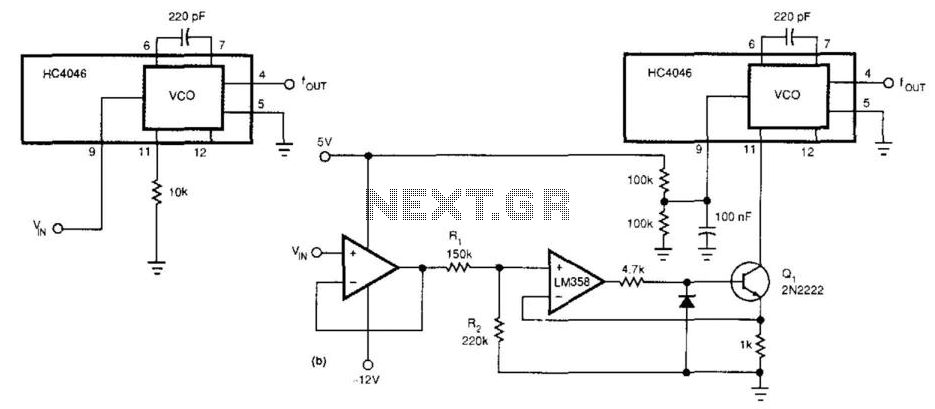
This circuit expands the linear frequency range of an HC4046 from one decade to nearly three decades. An LM358 is utilized as a constant-current sink, replacing the frequency-determining resistor (10 kΩ) connected from pin 9 to ground. For this...
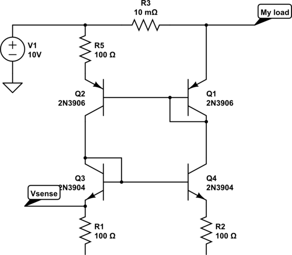
The bases and emitters of the transistors are connected together, resulting in equal base-emitter voltages. Assuming the transistors are identical, equal Vbe leads to equal base currents, which in turn results in equal collector-emitter currents. By adjusting the voltage...
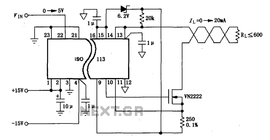
The circuit depicted in the figure consists of an ISO113 current loop isolation drive circuit that operates with an input signal (VIN) to provide an isolated amplified output of 0 to 20 mA. This current is transmitted to the...
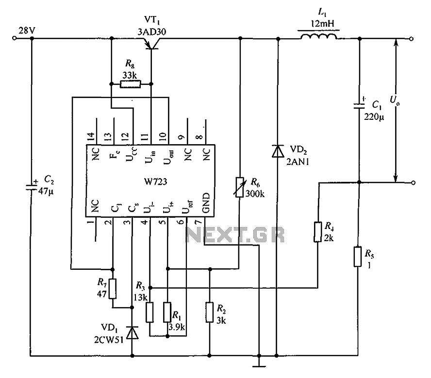
The Multiport W723 is an adjustable constant current regulator designed for use in switching regulator circuits, capable of delivering an output current of 1A. In the illustrated circuit, the W723 reference base voltage is approximately 7.2V. This voltage is...