
Voltage-to-frequency-converter

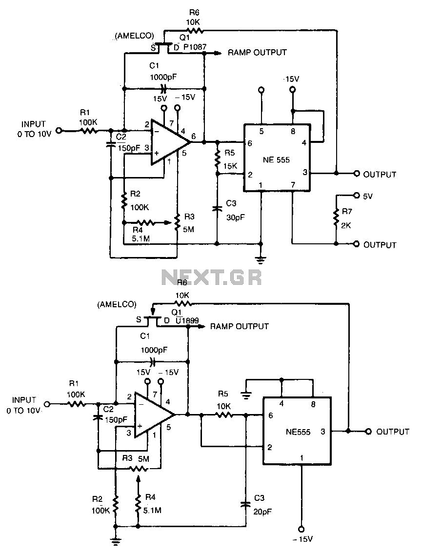
This circuit utilizes a 741 operational amplifier (op-amp) and a NE555 timer configured in astable mode to generate a frequency output based on control voltages. The operational amplifier functions as a current source, where the output current is modulated by the input voltage Ec. This current charges the timing capacitor C1 at a linear rate, which is critical for establishing the timing intervals in the NE555 timer configuration.
The NE555 timer in astable mode continuously switches between its high and low states, producing a square wave output. The charge and discharge cycles of capacitor C1, influenced by the control voltage, dictate the frequency of the output waveform. The operational amplifier's output is designed such that when the control voltage is zero, the output frequency is also zero, ensuring a direct correlation between the control voltage and frequency output.
The circuit features a 10-kilohm potentiometer that allows for fine-tuning of the offset voltage, ensuring that the system operates correctly at zero frequency when no control voltage is applied. The specified frequency of 4.2 kHz is achieved with particular component values, which can be adjusted as needed for different applications.
Furthermore, the circuit's design allows for the application of two DC voltages across resistors R1 and R4. The difference between these two voltages directly influences the output frequency, making this circuit suitable for applications requiring frequency modulation based on varying voltage levels. This characteristic is particularly useful in signal processing and control systems where precise frequency outputs are necessary based on differential voltage inputs.This circuit can accept positive or negative or differential control voltages. The output frequency is zero when the control voltage is zero. The 741 op amp forms a current source controlled by the voltage Ec to charge the timing capacitor C1linearly. NE555 is connected in the astable mode. so that the capacitor charges and discharges between 113 Vee and 213 Vee· The offset is adjusted bY the 10-K potentiometer so that the frequency is zero when the input is zero. For the component values shown: f = 4.2 Ee kHz. If two de voltages are applied to the ends of R1 and R4, the output frequency will be proportional to the difference between the two voltages.
Related Circuits
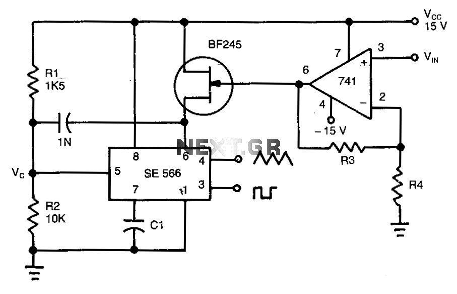
This circuit operates based on the frequency variation of the function generator in relation to the input voltage (ViN). The frequency is influenced by the capacitance and resistor connected to pin 6, with the resistor being substituted by a...
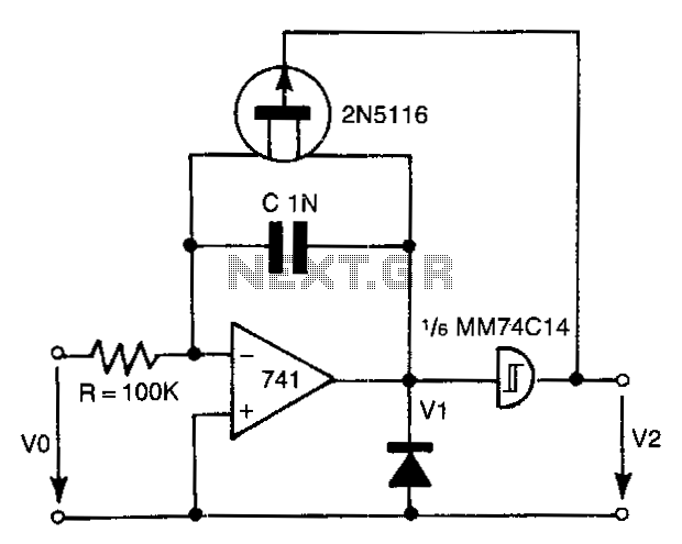
The 741 operational amplifier integrator signal is input into the Schmitt trigger of an inverter. When the signal reaches the positive-going threshold voltage, the inverter's output switches to zero. This output directly controls the FET switch. With a gate...
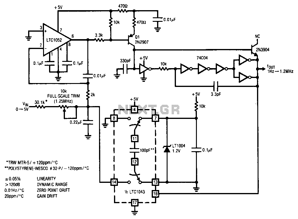
This stabilized voltage-to-frequency converter operates within a range of 1 Hz to 1.25 MHz, featuring a linearity of 0.05% and a typical temperature coefficient of 20 ppm/°C. The circuit is powered by a single 5-V supply. It employs a...
This linear voltage-to-frequency converter achieves good linearity over the range of 0 to -10 V. Its mirror image provides the same linearity over the range of 0 to +10 V; however, it is not compatible with DTL or TTL. The...
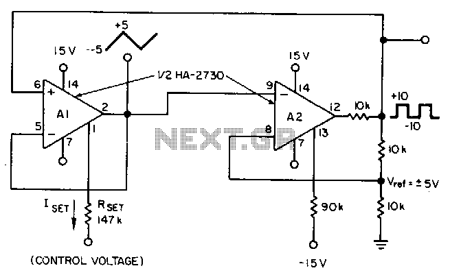
This circuit utilizes a programmable operational amplifier, specifically the HA2730, which is a two-amplifier monolithic chip featuring independent programming ports for each amplifier. The parameters of the amplifiers, including the slew rate, vary linearly based on a set current....
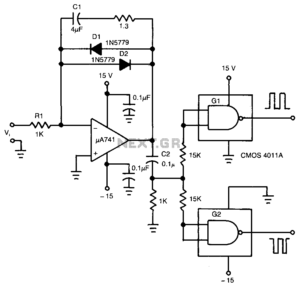
The input voltage, V1, causes capacitor C1 to charge, producing a ramp voltage at the output of the 741 operational amplifier. Diodes D1 and D2 are four-layer devices. When the voltage across C1 reaches the breakover voltage of either...