
Voltage-To-Frequency Converter Ii
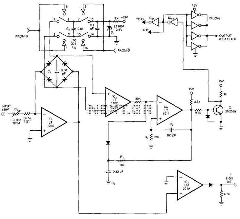
The voltage-to-frequency converter (VFC) is designed to convert bipolar AC voltages ranging from -10 V to +10 V into a frequency output that varies from 0 kHz to 10 kHz. The core of the circuit utilizes a combination of operational amplifiers, comparators, and a charge pump to achieve accurate frequency conversion with minimal distortion and high linearity.
The circuit begins with a bipolar square wave input, which is processed by operational amplifier IC1. During the positive phase of the input, IC1 generates a negative output that drives current through capacitor C1 via a full-wave diode bridge configuration. This arrangement ensures that the current flow is unidirectional, allowing for a linear ramp-up of voltage across C1 as a function of the input signal. The linearity of the output is maintained at an impressive 0.04%, ensuring reliable performance across the specified input range.
The instrumentation amplifier IC2 is configured with a gain of 10, allowing it to amplify the differential voltage across C1 for further processing. The output from IC2 is critical, as it serves to bias the negative input of the comparator IC3. When the output from IC2 crosses zero, IC3 is triggered to provide positive feedback to its own positive input, effectively latching its output state for a brief duration of approximately 20 µs. This feedback mechanism is essential for creating a stable frequency output that corresponds to the input voltage.
The level shifter Q1 is employed to drive two ground-referred inverters, IC5A and IC5B, which generate a biphase drive signal for the charge pump IC6 (LT1004). The charge pump is responsible for periodically discharging capacitor C2 across C1, effectively resetting its voltage to a lower level. The amount of charge removed during each cycle is determined by the reference diode D1 and the capacitance value of C2. This process is crucial for maintaining the oscillatory behavior of the circuit, as it allows IC1 to recharge C1 each time the output from IC2 attempts to cross zero.
The frequency of oscillation generated by the VFC is directly proportional to the current derived from the input signal, ensuring that the output frequency accurately reflects the input voltage level. The circuit's operation is symmetrical for both positive and negative input excursions, with IC2 detecting the same differential signal regardless of the input polarity. Additionally, IC4 plays a vital role in monitoring the output polarity of IC1, providing a bidirectional output signal that can be utilized for further processing or interfacing with other circuit components. This comprehensive architecture enables the voltage-to-frequency converter to deliver precise frequency outputs in response to varying bipolar AC inputs. This voltage-to-frequency converter (VFC) accepts the bipolar-ac inputs. For -10- to + 10-V inputs, the c onverter produces a proportional 0- to 10-kHz output. Linearity is 0.04%, and temperature coefficient (TC) measures about 50 ppm/°C. To understand the circuit, assume that its input sees a bipolar square wave. During the input"s positive phase, ICl"s output swings negative and drives current through CI via the full-wave diode bridge. ICl"s current causes Cl"s voltage to ramp up linearity. Instrumentation amplifier IC2 operates at a gain of 10 and measures the differential voltage across CI.
IC2"s output biases comparator IC3"s negative input. When IC2"s output crosses zero, IC3 fires ac positive feedback to IC3"s positive input and hangs up IC3"s output for about 20 /as. The Q1 level shifter drives ground-referred inverters IC5A and IC5B to deliver biphase drive to LT1004 switch IC6.
IC6, configured as a charge pump, places C2 across CI each time the inverters switch, which resets CI to a lower voltage. The LT1004 reference (Dl), along with C2"s value, determines how much charge the charge pump removes from CI each time the charge pump cycles.
Thus, each time IC2"s output tries to cross zero, the charge pump switches C2 across CI, which resets CI to a small negative voltage and forces IC1 to begin recharging CI. The frequency of this oscillatory behavior is directly proportional to the input-derived current into IC1.
During the time that CI is ramping toward zero, IC6, places C2 across the reference diode (Dl), and prepares C2 for the next discharge cycle. The action is the same for negative-input excursions, except that ICl"s output phasing is reversed. IC2, looking differentially across ICl"s diode bridge, sees the same signal as it does for positive inputs; therefore, the circuit"s action is identical.
IC4, detecting ICl"s output polarity, provides a signal bid output. 🔗 External reference
Related Circuits
S/PDIF is an acronym for Sony /Philips Digital Interface (or Sony /Philips Digital Interconnect Format). The full specification for the S/PDIF interface consists of hardware and software, but only the hardware side will be discussed here - the software...
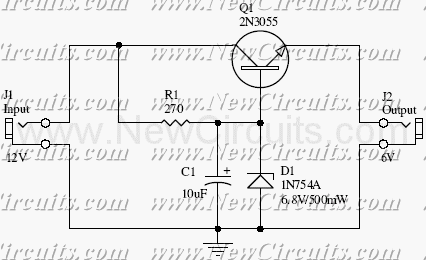
This small but useful circuit is a DC voltage converter for using 6V devices with car battery voltage. The maximum output current is dependent if the T1 is covered with a proper heat sink or not. You can use...
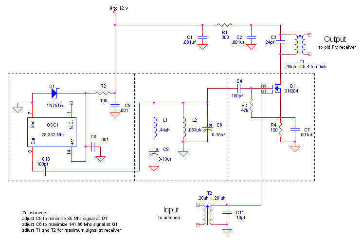
Here is my design for a modern receiving converter for pre-war FM sets. Accordingly, this article presents a design for listening to present day FM stations on a prewar FM set based on a MOSFET transistor and a TTL...
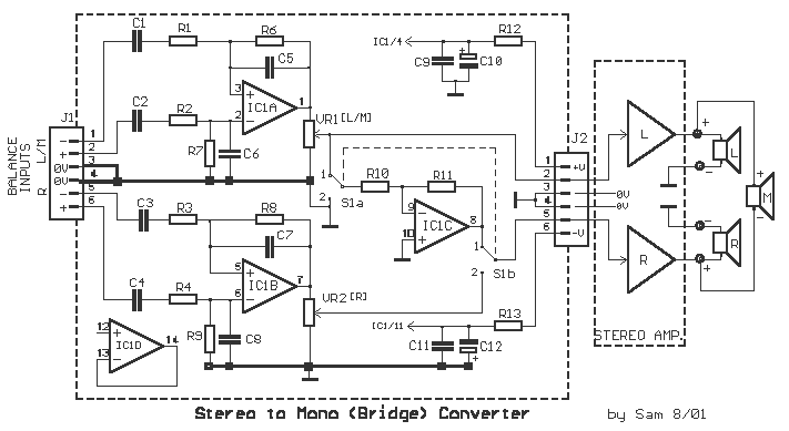
This is a very useful circuit for those who want to transform a stereo Power Amplifier to mono, bridging two channels from it, reversing the phase of one power amplifier [R] and the polarity. With these connections, it is...
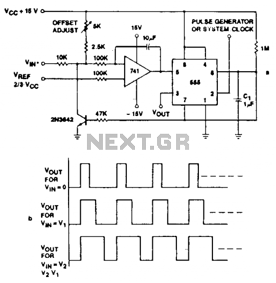
Accuracies better than 1% can be achieved with this circuit (a), and the output signals (b) maintain the original frequency, regardless of the input voltage. Voltage levels can be transformed into pulse durations by integrating an operational amplifier (op...
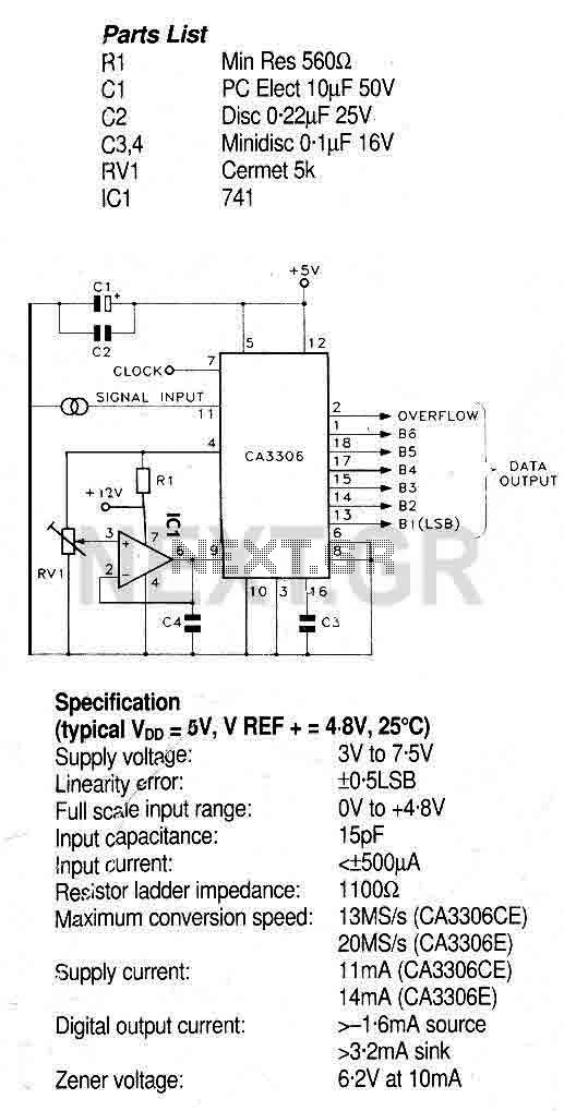
This circuit utilizes the CA3306, a family of CMOS parallel (flash) analog-to-digital converters designed for low power and high-speed applications. The CA3306CE operates at sampling rates of up to 10 million samples per second, while the CA3306E can achieve...