
XR2212 PLL FM demodulator Circuit
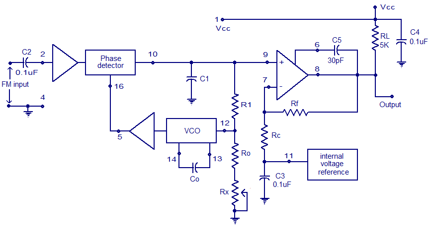
The PLL FM demodulator circuit utilizing the XR2212 integrates several key components that work in unison to achieve effective frequency demodulation. The phase-locked loop architecture consists of a voltage-controlled oscillator (VCO), a phase detector, and a low-pass filter. The VCO generates a frequency that is locked to the incoming FM signal, ensuring that any changes in the frequency of the FM signal are tracked accurately.
The phase detector compares the phase of the incoming FM signal with the output from the VCO. When these two signals are in phase, the output of the phase detector is minimal, indicating that the loop is locked. However, when the frequency of the FM signal deviates due to modulation, the phase detector produces an output that corresponds to this deviation. This output is then processed through a low-pass filter, which removes high-frequency noise and allows only the desired modulation signal to pass through.
The filtered signal is then amplified to a suitable level for further processing or output. The amplification stage is crucial, as it ensures that the demodulated signal maintains a sufficient amplitude for the next stage of the signal chain. The final output is a demodulated signal that accurately represents the original information encoded in the FM carrier wave.
In summary, the XR2212 PLL FM demodulator circuit effectively demodulates frequency-modulated signals by leveraging the principles of phase locking. The combination of the phase detector, low-pass filter, and voltage-controlled oscillator facilitates a robust and stable demodulation process, making this circuit an excellent choice for various communication and control applications.A simple PLL FM demodulator circuit using IC XR2212 is shown here. XR2212 is a highly stable, monolithic PLL (phase locked loop) IC specifically designed for communication and control system applications. The IC has 0. 01 Hz to 300KHz frequency range, 4. 5 to 20V operating voltage range, 2mV to 3Vrms dynamic range, high temperature range, TTL / CMOS compatibility and adjustable tracking range. The operating of a PLL FM demodulator is incredibly simple to know. The input FM signal and the output of the VCO is applied to the part detector circuit. The output of the part detector is filtered employing a low pass filter, the amplifier and then used for controlling the VCO. When there`s no carrier modulation and the input FM signal is in the center of the pass band (i. e. carrier wave only) the VCO`s tune line voltage are going to be at the middle position. When deviation in carrier frequency happens ( that means modulation occurs) the VCO frequency follows the input signal so as to keep the loop in lock.
As a result the tune line voltage to the VCO varies and this variation is proportional to the modulation done to the FM carrier wave. This voltage variation is filtered and amplified in order to get the demodulated signal. 🔗 External reference
Related Circuits
This source is selected by pressing a momentary-contact pushbutton switch (SI). Switch SI is connected to the trigger of a 555 oscillator/timer (U1) configured as a monostable multivibrator, which generates one short output pulse for each press of SI....
In audio systems, noise signals are generally undesirable, and efforts are often made to eliminate them. Transistors can be utilized effectively for this purpose due to their availability and low noise characteristics. The following circuit serves as a Noise...
The circuit diagram of a TV antenna is sourced from the technical information provided by Chinaicmart. For more detailed information or additional circuit designs, further inquiry may be necessary. The circuit diagram for a TV antenna typically consists of several...

How to create a Joule Thief circuit to power a clock, including circuit details and tips for construction. The Joule Thief circuit is a simple and efficient boost converter that allows the extraction of usable voltage from low-voltage sources, such...

This circuit generates a siren sound when switch S1 is pressed. The sound frequency increases as capacitor C1 charges, and when switch S1 is released, the frequency decreases as capacitor C1 discharges. The circuit operates on a simple principle of...
The AC power supply circuit primarily consists of a power supply, a reference voltage, a voltage comparator for sampling, and several other components. It includes a transformer for the input, an autotransformer tap for the control power supply circuit,...