
Z80 clock circuit
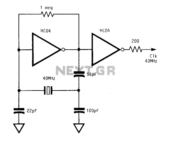
The described circuit functions as a high-frequency oscillator capable of generating signals across a wide frequency spectrum, from sub-MHz to over 400 MHz. The use of a 5 V supply voltage ensures that the output from the second inverter reaches the maximum logic levels, providing reliable high and low states essential for digital logic applications. This characteristic is particularly beneficial for interfacing with various digital components, including microprocessors, microcontrollers, and other peripheral devices that require precise timing signals.
To enhance the performance of the oscillator and mitigate potential signal integrity issues, a damping resistor is implemented in series between the oscillator's clock output and the input of the driven device. This resistor serves a critical function by attenuating any high-frequency noise, undershoot, or ringing that may occur due to the fast switching characteristics of CMOS technology. By smoothing out these transients, the damping resistor helps maintain signal fidelity and ensures that the receiving device interprets the clock signal accurately.
In designing this circuit, careful consideration should be given to the value of the damping resistor. An appropriate resistor value must balance between sufficient damping to eliminate ringing and undershoot while not excessively slowing down the signal rise and fall times. This balance is crucial for maintaining the overall performance of the circuit, particularly when interfacing with high-speed digital components.
Overall, this oscillator circuit represents a robust solution for generating high-frequency clock signals, with the added advantage of signal integrity enhancement through the use of a damping resistor. Its wide frequency range and compatibility with various digital devices make it a versatile choice for numerous electronic applications.The circuit will operate reliably from below 1 MHz to above 400 MHz. With Vcc = 5 V the output of the second inverter essentially attains a full swing from 0 V to 5 V. Such large logic output levels and broad frequency range capabilities make this oscillator quite suitable for driving MOS components such as CPU, controller chip, peripheral devices, as well as other TTL products. A damping resistor in series between the clock output of the oscillator and the input of the device being driven will remove the undesirable undershoot and ringing caused by the high speed CMOS part. 🔗 External reference
Related Circuits
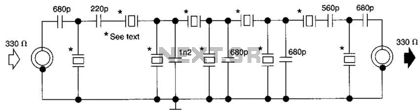
This filter utilizes five 455-kHz ceramic resonators. The impedance is 330 ohms, the bandwidth is 800 Hz, and the ultimate rejection is greater than 60 dB. Additionally, the ceramic resonators can be substituted with crystals. The described filter is a...
This Korean SuperCap OEM supports usage in series configurations. Consider whether the implementation will be manual or automatic, such as with a smart battery charger or a power fail backup circuit. It is essential to balance the voltage and...

This is a BTL (bridged tied load) mono amplifier with a DC volume control circuit. This circuit utilizes the TDA7052A/AT, which is suitable for monitors, TVs, and battery-operated portable radios and recorders. Unlike conventional DC volume circuits, the TDA7052A/AT...
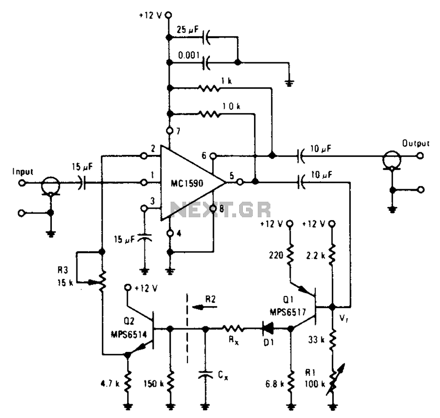
An amplifier designed to achieve a voltage gain of approximately 20, utilizing the MPS6517 PNP transistor in the emitter follower configuration. The RI controller allows for adjustment of the transistor's quiescent point. The output signal is activated only when...
The finger, positioned within a light screen, is situated between a high-intensity LED emitter and a photocell. It generates a heartbeat signal that, when appropriately amplified, serves as the input for a PIC16F84 microcontroller. The microcontroller drives three common...
This method of automatic level control (ALC) utilizes digitally switched audio attenuators within the signal path. The output level of the system is monitored, compared to a reference level, and audio pads are introduced through analog switches. This technique...
Warning: include(partials/cookie-banner.php): Failed to open stream: Permission denied in /var/www/html/nextgr/view-circuit.php on line 713
Warning: include(): Failed opening 'partials/cookie-banner.php' for inclusion (include_path='.:/usr/share/php') in /var/www/html/nextgr/view-circuit.php on line 713