
Speech compression circuit diagram
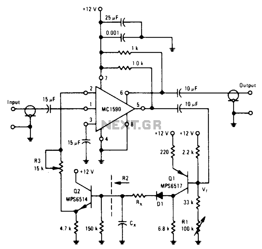
The amplifier circuit operates by leveraging the characteristics of the MPS6517 PNP transistor in an emitter follower configuration, which provides a high input impedance and low output impedance, making it suitable for driving loads. The voltage gain of approximately 20 indicates that the output voltage is 20 times the input voltage, allowing for significant amplification of weak signals.
The RI controller plays a crucial role in setting the static operating point of the transistor, ensuring optimal performance. By adjusting the quiescent point, the circuit can accommodate varying signal levels and maintain linearity in amplification. The reference voltage Vr, set at 7.0V, serves as a threshold that must be surpassed for the diode D1 to conduct. This feature prevents the amplifier from responding to noise or low-level signals, thus enhancing the signal-to-noise ratio.
When the input signal's peak exceeds the reference voltage Vr, diode D1 becomes forward-biased and conducts, allowing the positive peaks of the signal to pass through. This rectification process is essential for converting the AC signal into a usable DC output. The subsequent filtering stage, which includes capacitor Cx and resistor Rx, smooths the output signal, removing unwanted fluctuations and providing a stable voltage level.
The resistor Rx is particularly important as it determines the charging and discharging time constants for capacitor Cx. A larger resistance value will result in a longer time constant, leading to slower charging and discharging of the capacitor, which can be beneficial for applications requiring a gradual response. Conversely, a smaller resistance value will lead to a quicker response, making the circuit more reactive to changes in the input signal.
In summary, this amplifier circuit effectively manages signal amplification and processing through careful design considerations, including the choice of transistor, the implementation of a quiescent point adjustment mechanism, and the incorporation of rectifying and filtering components. These elements work together to ensure reliable performance in various electronic applications.Amplifier capable of driving a voltage gain of about 20 MPS6517 PNP type emitter electrode group is. RI controller can change the static point of the transistor Q, which is to change the quantity exceeds the signal level Vr. Only when the peak is greater than Vr when (Vr F7.0V), the output of the diode D1 can be rectified positive peaks Q1. The resulting output filters Cx and Rx. Rx control the charging time constant or time out. Charging and discharging are required to use Cx.
Related Circuits
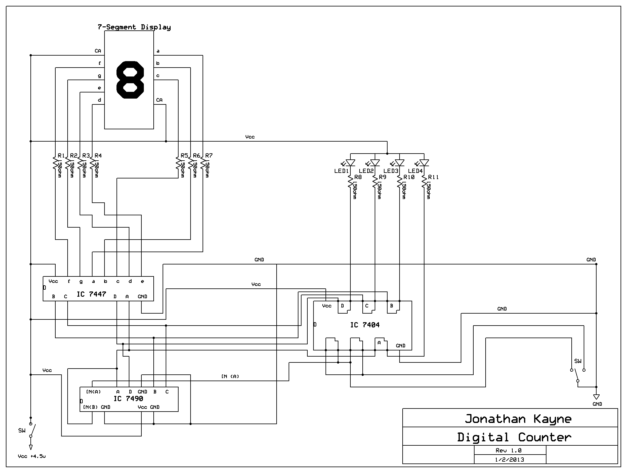
The Digital Counter Circuit is an electronic project that converts digital numbers (0-9) to binary (0-1). For those interested in understanding binary code, a PowerPoint presentation on the topic is available. Below are the parts list, schematic, and additional...

The circuit is constructed using the ICM7217 integrated circuit from Intersil, which features a CMOS up/down counter with a four-digit display. The clock generator circuit, IC3, produces a square wave clock signal with a period of one second, available...
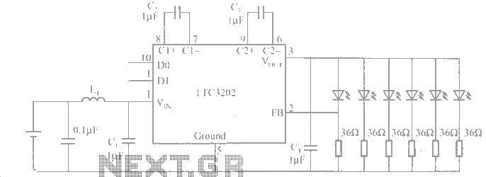
The LTC3202 is a device from Linear Technology that eliminates the need for a charge pump gated oscillator. It is designed as a charge pump for driving white LEDs powered by a lithium-ion battery. To address noise issues, the...
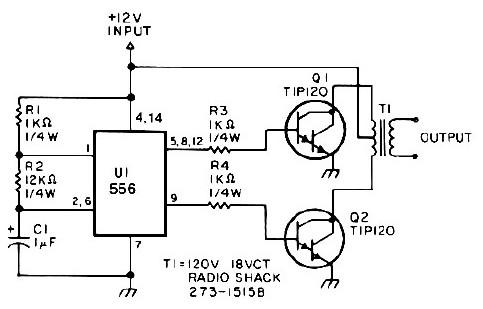
This low-power 25-watt power inverter circuit utilizes only nine electronic components. The inverter converts a DC input voltage ranging from 10V to 16V into a 60Hz, 115V square-wave power output, capable of powering AC electronic devices up to approximately...
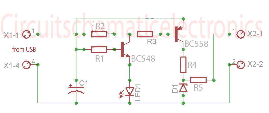
Without a USB to phone battery charger circuit, charging a phone battery using a USB port on a computer can quickly damage the battery, resulting in bulging. This occurs because the voltage output from USB is 5 volts, while...
Fire alarm circuit using an LDR (Light Dependent Resistor) as a flame sensor. It warns the user about fire accidents by detecting smoke produced during a fire. As smoke passes between an LED and an LDR, the amount of...